
A Comprehensive Primer on Advanced Semiconductor Packaging
Your ultimate guide to almost every concept you will ever need to know about how chips are packaged and how the future of interconnect technology is shaping up.

The world of semiconductor packaging is complex and diverse, and with the increasing trend of silicon disaggregation into chiplets and heterogenous integration, is also highly relevant. For a gentle introduction to chiplets, read this excellent guide by Austin Lyons.
The problem I encountered when doing the research for this post is the confusing marketing terminology used by players in the industry. Every vendor uses a different name for the same technology. This makes it hard to separate the concepts from the brand names. I’m guessing I may not be alone here. A good starting point for me is SemiAnalysis’ five-part series on advanced packaging (link in references) which discusses a mix of technology and business.
In this long post, I attempt to focus on just the conceptual aspects of packaging technologies and their evolution. Several of the recent advances in packaging technologies and the materials/processes that enable them are active areas of research and won't be covered here in detail. This post will focus more on the interconnect assembly/scaling aspects of packaging versus other increasingly important functions of a package like power delivery, signal integrity or thermals. I have also intentionally not covered niche packaging technologies involving optics and MEMS.
The semiconductor packaging world just in itself has a whole lot more than I can reasonably cover even in a post as long as this; my apologies in advance if I left out something important. Please comment or reply to this email and let me know what other important aspects I should cover in the future.
Big thanks to Bharat Penmecha for his detailed review, edits, and additions to this post.
Bharat has over a decade of experience developing 2D, 2.5D, 3D advanced packaging technologies and bringing products to market in Datacenter, FPGA, Client, Automotive, Edge and Networking segments . His skillset spans thermomechanical simulations, materials, process flows, and packaging architecture definition.
One quick thing: This post is completely free for all subscribers because I think the contents are important for anyone interested or working in semiconductors. If you find this information useful in your work or education, please consider upgrading to a paid subscription. I’m always grateful for your support!
Check out the discounts section for student and purchasing parity pricing. Also, see the benefits of a paid subscription.
Here is what we will cover:
2D: Flip-chip technology: overview, process and copper pillars
2D: Wafer level packaging: RDL, chip-first, chip-last, panel-level fan out
2.5D: Silicon interposers, micro-bumps, TSVs and silicon bridges
Here is a visual guide to most of the packaging types we will discuss in this article.

Read time: ~30 minutes.
Introduction to Electronic Packaging
Chips are made on silicon and are useless until they can be interfaced with the external world. Connections for signals, ground, or power are usually made via pads on the chip, and depending on the electrical performance and form-factor required, the interconnection can take many forms.
Electronic packaging is the process of:
Enclosing a semiconductor device to protect the sensitive circuits on it from external elements.
Making proper interconnections and interfaces between the circuit and other semiconductor devices or the outside world, with the intent of delivering power, connecting signals or transferring heat.
While packaging serves several extrinsic purposes as highlighted above, an intrinsic purpose is the length scale transition it offers from 10-100s of microns at the chip bump level to millimeter-centimeter scale at the board level; it acts as a length scale transformer.
Depending on the type of package used to enclose a chip, the packaging process can be performed by semiconductor foundries themselves (also called Integrated Device Manufacturers, or IDMs), or externally at Outsourced Semiconductor Assembly and Test (OSAT) facilities. OSAT facilities are responsible for manufacturing the package, assembling the chip, and testing it to ensure functionality. Majority of the OSATs are concentrated in the southeast Asia region, where some notable examples are ASE, Amkor and JCET (StatsChipPAC). If you want to delve deeper in how OSATs work, I recommend this article.
In an ideal world, the package should have no impact on the electrical properties of the enclosed silicon chip. This is never the case. The leads of the package and the internal connections between the chip and the package affect the electrical performance of the silicon chip. As transistors have gotten smaller and the quantity and rate of data interchange between chips in a system has exploded, packaging has become a major bottleneck on system performance. The need to minimize the electrical penalty of chip packaging has become more critical than ever.
Transistors have reasonably kept up with Moore’s law with counts roughly doubling every two years. But the density of packaging interconnects has significantly lagged behind. Chip designs are said to become pad-limited when the packaging technology is not dense enough to provide interconnections to the increasingly dense transistors on a chip. When this happens, chip makers add more functionality on the chip like extra SRAM to ensure that the overall chip size is big enough for the package to connect to. While this has system benefits, it is not sustainable in the long run due to the increasing cost of silicon on advanced technology nodes. With the emergence of chiplet technology, sophistication in electrical packaging is more relevant than ever.

In the next section, we will look at how packaging technology started out, and eventually see how the complexity of chip packaging has evolved to where it is today.
The Early Days
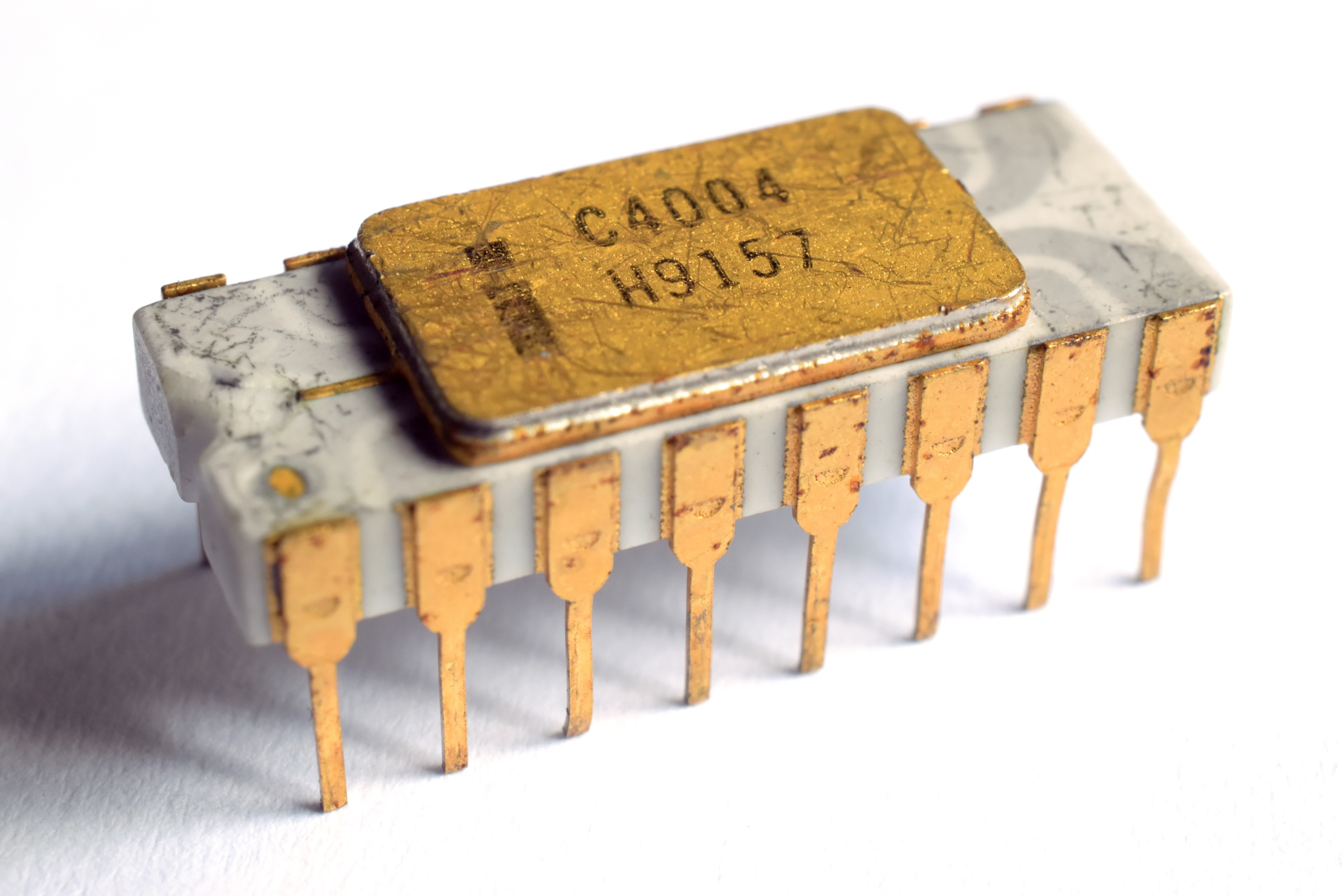
The earliest forms of packaging in the 1970s and 1980s used a Dual-Inline-Package (DIP) which essentially consisted of an L-shaped leadframe and a central paddle onto which the silicon chip was mounted. The connection from the leadframe to the chip was made with tiny metal wires called bondwires. The whole thing was then covered by a resin to mechanically protect the internals of the package. The leadframe was then soldered on to the printed circuit board which had through-holes in them.

The Intel 4004 CPU, which was the first example of large scale integration with 2,300 transistors released in 1971, used such a DIP package.
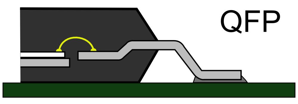
The protruding leadframe and the need for holes in the circuit board to integrate these packages were cumbersome, and so these gave way to Quad-Flat-Packages (QFPs) which had more of a ‘gull-wing’ leadframe, maintained a more flat profile and did not need holes in the circuit board. These were popular in the late 1980s and early 1990s. A famous example is the Zilog Z80 CPU which was released in both DIP and 44-pin QFP packages.
The next evolution was the Quad-Flat-No-lead (QFN) package which did away with the long leadframe pins completely and provided three advantages: reduced inductance, lower weight and profile, and a package size that was almost the same as the chip itself. The leadframe now was a single piece of metal which connected to the board on one side, and had a bond wire on the other connected to the chip. The reduced inductance enabled these packages to be used in high frequency designs for RF products (low-GHz range).
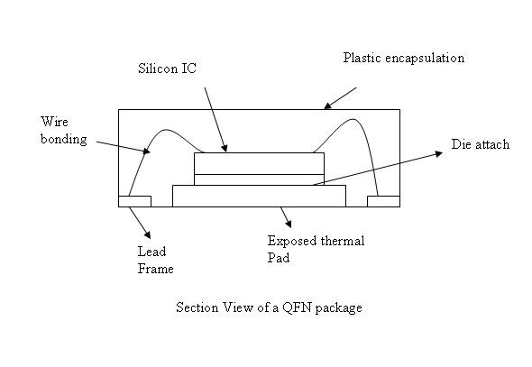
A noteworthy feature of the QFN package is its ability to conduct away heat from the silicon chip. The thermal conductivity of the paddle on which the chip is mounted is excellent and it can conduct away a large portion of the heat due to its large footprint. Even today, these packages still continue to be used in power, industrial and automotive applications where thermal dissipation is critical compared to size, complexity or high frequency operation.
There were also a host of other kinds of packages like thin small outline package (TSOP), leadless chip carrier (LCC) and a host of other variations on these designs. We will not cover all kinds of early packages; there are simply too many. While some of these are still being used today, the big leap ahead in packaging came from flip-chip technology.
2D: The Flip-Chip Package
In the 1990s, a new technology became the norm that is widely now regarded as a ‘step-function’ in the evolution of chip packaging called flip-chip. You may also come across this as controlled collapse chip connection, or C4. The basic idea was to eliminate the bondwire and create a new connection with just balls of solder. This marked the move to using the entire area of the chip to form package interconnects, rather than just the edges that wirebond enabled, there by providing more connections per chip. In the wire bond constructions, the metallization and the devices used to be in the “face-up” configuration, the C4 technology “flipped the chip”, making the metallization and devices face down.
Technology
For flip-chip packaging, solder balls are placed on the pads of the chip. This is done all at once on the entire silicon wafer that is up to 12 inches in diameter, in a process called bumping. The allowed space between bump centers was about between 130 and 200 microns, which is commonly referred to as bump pitch. Bump density expressed as number of bumps per square millimeter is also a common metric in the industry. The individual chips are then diced out of the wafer with their solder balls in place to be attached to a package substrate.

Modern package substrates comprise of an organic core material that accounts for the bulk of the substrate (some applications use a “Coreless” stackup.) This is commonly Flame Retardant 4, or FR4, a woven fiberglass material that is self-extinguishing. Subsequently, there are thin polymer dielectric films that are built up on either side of the substrate. Between the films, metal traces are deposited and vias (basically little interconnects that connect metals at different levels) are etched between films to form multiple metal layers on the substrate and are used for routing metal connections on the package. The most common film material used to build modern multi-layer packages is Ajinomoto Build-up Film (ABF) which is the same company famous for its MonoSodium Glutamate (MSG) product widely used for its umami taste. That’s an interesting story for an another day.

Unlike the popular dual damascene process used for the interconnect layers on silicon in the fabs, substrate manufacturing uses semi-additive-processing (SAP) where the dielectric films are laminated over existing metal features, inter-layer interconnect openings (for vias) are laser formed in the laminate layer and metal features of the next layer are electroplated.
Assembly Process flow
The singulated die with the solder balls is then turned upside-down, or flipped, onto the package. The chip and the package are carefully aligned to make good connection. In the conventional method of chip attach, heat is applied to reflow the solder balls — which simply means that the solder balls briefly melt to form a connection with the package due to high surface tension of molten solder and then harden again. But as die sizes get larger or the pitch of the interconnect is shrinking, thermal compression bonding technique is being increasingly employed.
The space around the solder balls (between the chip and package) is then filled with a capillary underfill (CUF) material. When temperature changes during chip operation, the chip and substrate to expand at different rates due to varying coefficients of thermal expansions (CTEs) creating stress on the joints. CUF provides much needed mechanical stability to keep the chip from detaching from the substrate.
Following this, the package goes through heat-spreader attach (if needed), package solder ball (Ball-Grid-Array, or BGA) attach and is ready for board level assembly.

There are a few advantages to flip-chip technology that are worth spelling out:
Low parasitics: Compared to bondwires in leadframe or QFN packages which were hundreds of microns long, the solder ball height is about 50-70 microns. This lowers interconnect resistance and inductance drastically and allows the package to be used for high performance applications.
Compact size: The chip and package sizes can be very nearly equal because the bondwire is eliminated. The overall packaged chips are therefore much smaller and lighter without those long leadframe metals used in DIP or QFP.
Multi-chip integration: The ability to create metal interconnects on ABF means that more than one silicon die can be placed on the substrate and connected through metal lines. This allows chips with various functionalities to be integrated together on a single package along two dimensions.

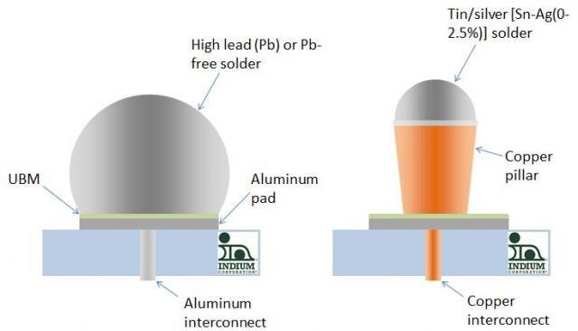
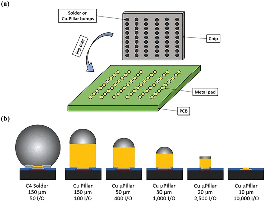
Reducing bump pitch with copper pillars
As the device sizes on silicon continued to scaled down, transistor count increased and the number of signals coming out of the chip went up. There was a need to provide more interconnect bumps per unit area of the chip which was achieved by making the pitch and size of the bumps smaller.
The spherical shape of solder bumps is undesirable if the bump pitch needs to get smaller. When copper pillars with a solder cap on top replaced solder bumps, the bump pitches dropped below 100 microns. The cylindrical shape of copper pillars meant that you could put them closer and further bump pitch improvements could be made by reducing the diameter of the copper pillars.
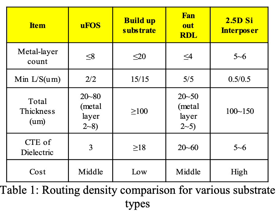
The table below from the 2024 Heterogeneous Integration Roadmap predicts that flip-chip bump pitches will not go much below 90 microns on standard core packages because they are limited by the line/space (L/S) feature sizes that are possible to manufacture on standard packaging substrates. This seems reasonable because going below these bump pitches means that you will need fine-pitch technologies like micro-bumps and substrates that support finer features like interposers. We will discuss these later.

2D: Wafer-Level Packaging
Instead of making the package separately and then attaching the chip to it via flip-chip assembly, wafer-level packaging is a different evolution of the packaging flow that builds the package onto the chip while still in wafer form. Here is how it works.
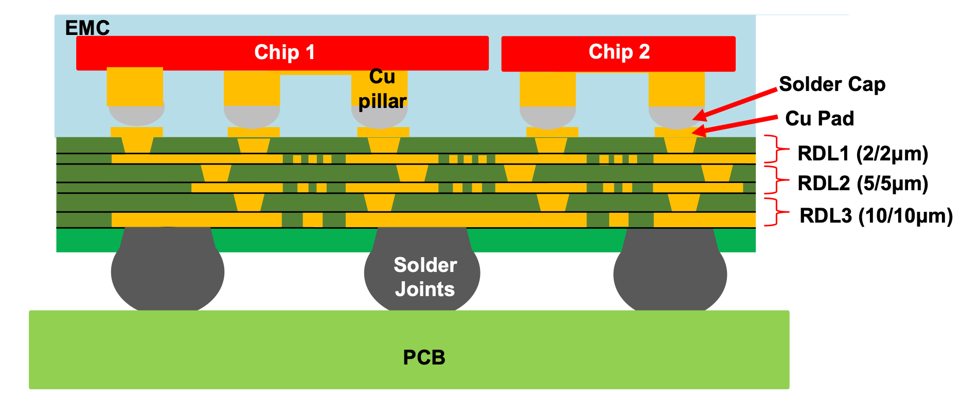
Like in flip-chip packaging, the chips are fabricated in a silicon process and diced from the finished wafer. The known-good diced chips are then placed the right side up (not flipped) onto a blank wafer often called a reconstituted wafer which is then covered with a dielectric mold layer. Excess mold is ground back to reveal the copper bumps on the chips, or via-holes are made in the mold layer wherever connections need to be made to the chip pads, and then metal lines are built on top of the dielectric. This interconnect layer formed on top of the chip is called the Redistribution Layer (RDL). The wafer then proceeds to the bumping step.

By building an RDL layer, you are no longer bound by the bump pitch of the packaging technology like in the case of flip-chip. The spacing of the chips on the reconstituted wafer can be made higher to build packages that are bigger than the chip itself. By ‘redistributing’ the chip connections over a larger area, there is now more room to place solder balls or copper pillars on the RDL layer.
RDL interconnect features are not as fine as on-chip metallization. L/S values of 10/10 microns are quite common, with high-end RDL technology being down to L/S of 2/2 microns. There could also be multiple RDL metal levels making complex routing possible. The packaging technology is not restricted to one type of chip; two different chips performing different functions on different process nodes can be packaged together and hooked up with RDL interconnects.
Ultimately, the chip(s) with RDL interconnect is diced out of the reconstituted wafer and flipped on to a PCB substrate as shown below.
The chip connections are said to fan-out over a larger area thereby simplifying the packaging process which is why it often called Fan-Out Wafer-Level Packaging (FOWLP) or Wafer-Level Chip Scale Packaging (WLCSP). This short 2.5-minute video visually explains the process well.
In scenarios where the signal, power/ground solder ball counts needed are small and can fit within the area of the die, wafer scale RDL process can produce a package at the same size of the chip or incrementally larger, saving space and cost in edge and mobile applications. This is called wafer-level fan-in packaging.
In wafer-level packaging, there are several process flows that are possible:
Chip-first: This is the process flow we just discussed where the chips are mounted on a reconstituted wafer and then the RDL layers are processed on it. Once the RDL layers are built on the wafer, the chip(s)+package is diced out of the reconstituted wafer. While this is a low-cost approach, there are downsides. During RDL processing, the die can shift out of place or get misaligned, and larger chips can warp. This limits chip-first technique to simpler packaging scenarios involving smaller die. Since known good die are committed upfront before fabricating RDL layers, it is imperative that the yield for the RDL process is very good to make it cost effective.
Chip-last: This process flow resembles the original flip-chip approach where the RDL is first formed on a reconstituted wafer and then the diced silicon chips are flipped onto the RDL interconnects and then molded. The advantage here is that the chips are not subject to the multiple thermal steps involved in RDL processing which keeps the original silicon chip intact. Since the RDL layers can be inspected/tested before assembling the die, yield loss due RDL defects can be avoided. This also allows finer features with L/S down to 2/2 microns to be patterned on RDL and results in better electrical performance. This packaging flow can be costlier due to additional assembly steps.
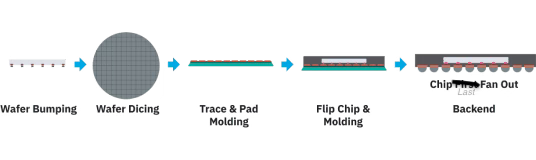
Chip-last fan out packaging. Image courtesy: ASE. Panel-level fan-out (PLFO): Both the above approaches use circular wafers which do not utilize area efficiently. Panel-level packaging involves using rectangular panels up to 600 mm x 600 mm instead of 300 mm diameter reconstituted wafers, which results in a much lower cost per package (up to 20%) due to high area utilization. This is still a relatively new technology which faces some hurdles. Manufacturing base and tool vendors need to upgrade their facilities and offerings to support large rectangular panels. The number of RDL levels currently supported is still evolving and the feature sizes are coarse. But for many applications such as power-management ICs, the current PLFO capabilities are sufficient and provide a low-cost, high volume wafer scale packaging solution.

Panel level packaging on a 600x600 mm2 panel provides 6.5x more packages on a single panel run. Image courtesy: StatsChipPAC.


There are further categorizations of these flows as face-up vs face-down chip placement which we won’t get into here.
The Rise of Advanced Packaging
While conventional packaging served its purpose well for several decades adapting to the changing needs of silicon, several new trends have emerged over the past decade which have made packaging an increasingly important component of electronic devices.
Disaggregation: With Moore’s law slowing down and large die sizes on leading node becoming increasingly expensive, there is a need to disaggregate a single large die into multiple smaller chips called chiplets.
Heterogeneous Integration: IP blocks don't always scale with silicon node and to save porting costs, it is desirable to have different blocks on different silicon nodes ideally suited for them, leading to a desire to mix and match chiplets on the package.
Memory Wall: With demand for memory bandwidth far outpacing prevailing bandwidth scaling, processors which need high memory bandwidth needed to integrate the memory as close to the compute as possible, ending up on the package. This gave rise to HBMs which couldn't be accommodated with traditional packaging.
Breaking Reticle limits: Applications such as AI and Cloud computing drive demand for more compute per package. Since the largest possible single die is limited by the reticle limit, there is a demand to be able to breakthrough this restriction by adding more chips and making them function as a single very large chip.
These critical needs lead to the emergence of a class of technologies, termed as Advanced Packaging. The following sections describe the various offerings under this umbrella.
2.1D/2.3D: Ultra-thin organic interposers
So far we have looked at chips flipped onto substrates with FR4 core and organic dielectric films on which traces were developed. We also looked at RDL-based packaging techniques that were processed using wafer-level flows. 2.1D/2.3D packaging technologies are the combination of both flip-chip and “RDL-like” techniques. Some offerings on wafer-level RDL processes that connect multiple die with fine L/S traces are also classified as 2.1D packaging.
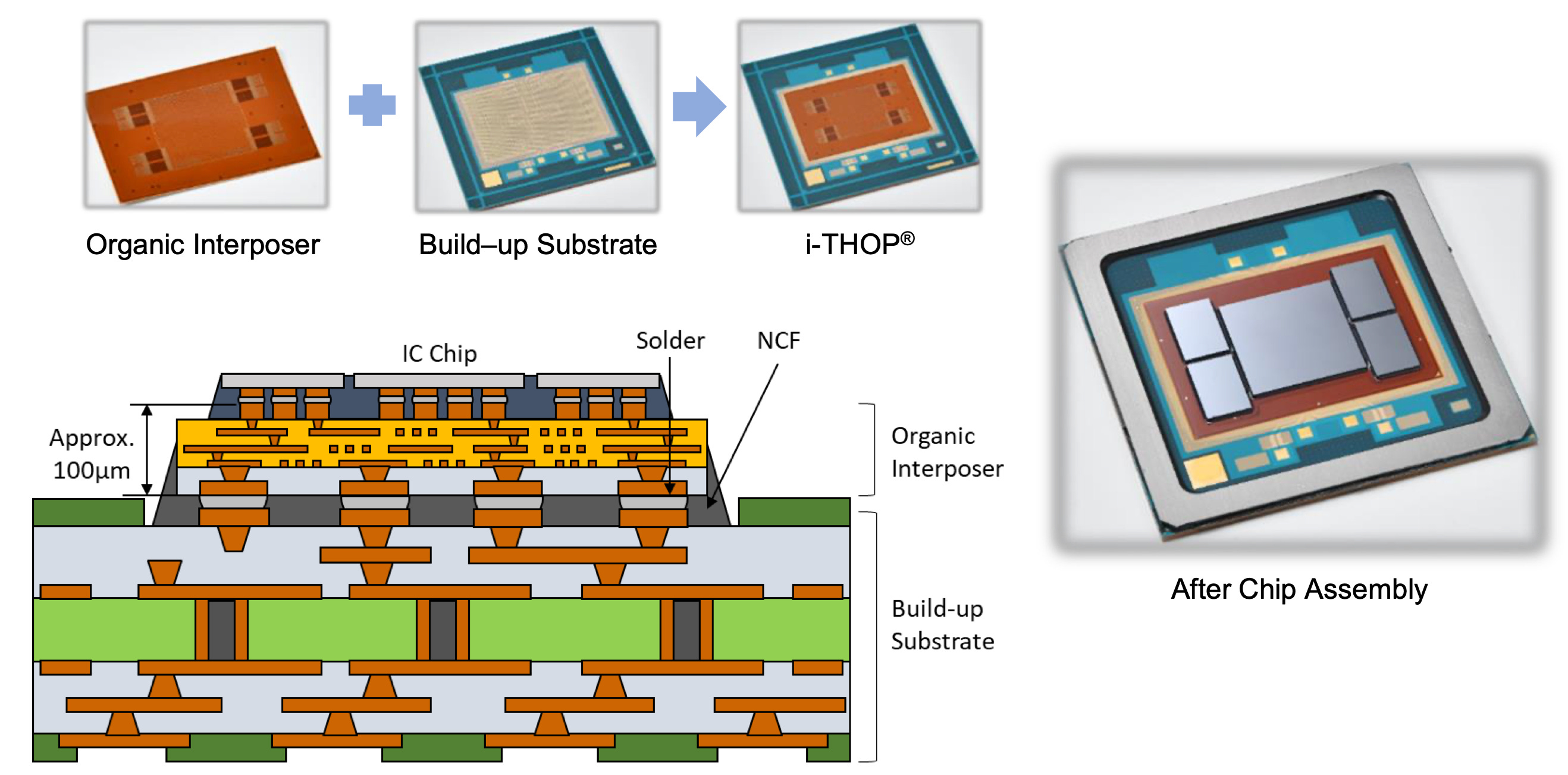
The “RDL-like” layer we are talking about here is an ultra-thin coreless substrate using polyimide-based organic materials in which multiple metal levels (8-10 layers) can be manufactured. Examples of such substrates are SHINKO’s i-THOP package or JCET’s ultra Fine-pitch Organic Substrates (uFOS). Such thin substrates, regardless of the material used, are often referred to as interposers. The main advantage of these ultra-thin organic interposers is that the metal feature sizes can be quite fine with L/S of 2/2 microns on all metal levels. This is particularly useful when the chips being integrated are developed in a modern process node where a lot of interconnections need to be made in a small area. The interposers are connected to the ABF film + Core FR4 substrate package using solder balls or copper pillars providing extra routing capability compared to the plain 2D package integration process we saw earlier.

The nomenclature of 2.1D/2.3D is to represent packaging technologies that are in-between 2D and 2.5D (which uses silicon interposers). There is no clear demarcation between 2.1D and 2.3D in itself; a lot of it is just loose marketing terms adopted by the industry.

2.5D: Silicon Interposers, Micro-bumps, TSVs and Bridges
If we want to further reduce the L/S and make smaller features on package for dense interconnects, we need to abandon organic interposers and go where small objects are best made — the silicon foundry. The term 2.5D is associated with packages that have a silicon chip combined with a passive silicon substrate (no active circuits involving transistors) that uses back-end of the silicon processing flow (hence the extra 0.5D.) We will discuss two kinds of 2.5D packaging: silicon interposers and multi-die bridges. We will also discuss interconnections on these technologies: micro-bumps and through-silicon-vias.
Silicon Interposers
The interposer itself is built on a silicon wafer using just back-end-of-line silicon processes to redistribute signals using metal interconnects. While no transistors are built on passive silicon interposers, passive components like capacitors can still be integrated into the RDL layer to create bypass capacitors (this can be done on organic interposers too.)
There are really three main advantages to using silicon interposers:
Feature sizes: L/S can be driven down to 0.5/0.5 microns on silicon interposer which enables some really dense interconnections for integrating chiplets.
Matching CTEs: Unlike wafer-level packaging or ultra thin organic substrate packaging that use materials other than silicon to build RDLs, the use of silicon as an RDL layer means that the coefficient of thermal expansion (CTE) between the die and interposer are matched. Using materials with compatible CTEs means that there are less manufacturing issues, warpage, stress and deformation in the packaging.
Through-Silicon Vias (TSVs): To connect the top of the silicon interposer to the bottom, via interconnects can be built right through the silicon. These are called through silicon vias (TSVs) and provide the shortest possible interconnect length between the chip and the external package. We will talk about TSVs in a bit more detail later.
Limitations of silicon interposers
The main downside of using silicon interposers is cost. The need for wafer fab equipment, however basic, is expensive to own, which limits silicon interposers to IDMs and foundries like Intel, TSMC and Samsung. OSATs do not manufacture silicon interposers themselves, but offer services to package them with chips.
The other limitation is interposer sizes are limited to the maximum reticle sizes that can be implemented on a 12 inch wafer — which is 858 mm². Making interposers larger than this area requires techniques like reticle stitching that makes the process expensive. This inherently limits the maximum length of interconnect that can be implemented on silicon. However, most leading foundries have perfected stitching process technology in x and y directions on the wafer and now offer interposers much larger than a single reticle with several products in mass production.
Glass is emerging as an alternative to silicon. Glass is lower cost, has low CTE and can be processed in rectangular panels instead of circular wafers in the case of silicon. Much like the panel-level packaging we looked at earlier, this brings down the unit cost of interposers developed on glass.
Micro-bumps
Due to the small metal line features that are fabricated on interposers to provide higher density, the chips that are flipped on to them often need to have finer bumping technology called micro-bumps. By scaling the diameter of the solder bumps down, micro-bumps have pitches well below 90 microns. For example, 50 micron bump pitches for use on interposer is common while state-of-the-art micro-bumping technology goes down to 10 micron pitch or lower. The graphic below shows the solder-on-copper microbumps along with the pitch the corresponding number of bumps expected per square mm.
Through Silicon Vias (TSVs)
So far, we have only made connections to the chip using pads on the upper metal layers of the chip on which wire bonds, solder balls, copper pillars or RDLs were built. The other method of connecting to a chip is from the bottom side using through-silicon-vias (TSVs), and there good reasons why this is useful.
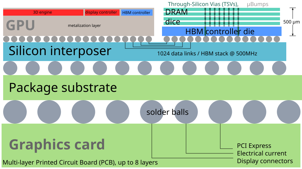
One of the most important applications for TSVs that is highly relevant today is High Bandwidth Memory (HBM), which is widely used in AI accelerators. Accessing contents of memory is critical to keep the GPU constantly fed with data, large amounts of which need to be accessed quickly to overcome the infamous memory wall.
The figure below shows the construction of HBM which involves vertically stacking multiple dynamic random-access-memory (DRAM) chips and connecting them together with microbumps. Each DRAM chip also has TSVs through it to connect to the chip above and/or below it.

HBM memory often has 8-16 stacked chips with each DRAM chip thinned to a thickness of 50-100 microns. TSVs used in latest HBM generations have a diameter of about 5 microns (a 10:1 aspect ratio) and a pitch of 30-50 microns. This allows a large number of parallel connections to be made on the HBM die, which is the primary reason for its high bandwidth.
TSVs can also be made on silicon interposers to make the shortest possible electrical connections between the chip and the package below it. Since interposers are usually 100-150 microns thick, TSVs used in interposers are often tens of microns in diameter to maintain a 10:1 aspect ratio or lower. The larger diameter of TSVs implies that their pitch is correspondingly larger — in the range of 20-100 microns. In 2.5D and 3D packaging TSVs perform the critical function of delivering power to the chips residing on the higher tiers and bringing out any signals onto the package, though they add some resistance to the path as their size shrinks.
At the other extreme of TSV technology is the use of nano-TSVs (nTSV) for backside power delivery networks on leading edge technology nodes. Intel’s PowerVia technology, for example, builds the power delivery network on the back of the silicon wafer so that low resistance connections using thick interconnect metals can be made to it, potentially avoiding power loss through metal resistance. TSMC also offers a similar technology which they call Backside Power Rail (BPR). The important feature of this technology is the use of nTSVs which can have a pitch of 5 microns or less, with nTSVs of diameters below 1 micron — representing the state-of-the-art in TSV technology.

Without going deep into TSV manufacturing flow, the important point to be made is the deep reactive ion etch (DRIE) process needed to make deep holes in the silicon substrate. It is termed the Bosch process and has alternating etch/passivation steps. It is usually a costly, time consuming process that makes TSVs expensive to manufacture even if it is for interposers. Depending on the application, the TSV can be made at different points in the fabrication flow:
TSV last: TSV is created after the entire chip is manufactured; often used in CMOS image sensors.
TSV middle: TSV is created after the process steps to create active devices such as transistors, but before back-end chip metals are formed; often used in 3DICs (discussed in next section) where the transistor performance should not be affected by the processing of TSVs.
TSV first: TSV is immediately created on the silicon substrate; ideal for silicon interposers where there is only metallization present.
Lastly, silicon interposers with RDL and TSV have also been used to integrate chips on both sides of the interposer as shown below, giving a high degree of integration.

Silicon Bridges
The reticle and wafer size limitations in silicon interposers restricts the total area of chips that can be connected with interposers. When combined with its inherently higher cost, silicon interposers are not the optimal solution for many advanced packages.
Silicon bridges are a unique packaging approach that combines silicon interposers and build-up substrates, to harness the benefits of both. Many foundries and packaging houses now support silicon bridges in their packaging flow, all with different marketing terminologies. We will understand the general approach even if each market player implements it slightly differently.
A silicon bridge is a miniaturized version of an interposer that for the large part eliminates TSVs to reduce cost (although some silicon bridges have TSVs too.) Once the silicon bridge is built, it is embedded into a cavity pre-formed in an organic buildup substrate and then chips are assembled on top. The lateral connections between adjacent chips are made through the bridges.
Since the footprint of each bridge is quite small, they are embedded in the substrate or organic interposer only where die-die interconnects are needed. The access to the chips sitting on top now, outside the bridge region, is directly though substrate vias or copper pillars which have much lower resistance compared to the TSVs of silicon interposers.
Let’s look at the process flow for Intel’s Embedded Multi-die Interconnect Bridge (EMIB) technology to understand the physical construction better.

First, the silicon bridge is manufactured in a silicon foundry using back-end process flow. The wafer is thinned and diced, ready for placement.
The organic package follows a conventional buildup process, up until the final buildup layer. At this point, an additional step is used to create a cavity in the substrate.
The bridge is placed inside the cavity and the final layers of dielectric in the buildup process are completed.
Fine vias are drilled in the dielectric where the chips will connect to the silicon bridge, and coarse vias are drilled elsewhere. The vias are metallized and planarized, and ready for flip-chip attachment of multiple silicon die which must be bridged.
Other than lower cost compared to silicon interposers, a notable advantage of silicon bridges is their modularity. They are not constrained by reticle size limitations like interposers because they are usually much smaller — only connecting the I/O interfaces of multiple chiplets in a system. This avoids the need for expensive approaches like reticle stitching that is often required to go beyond the reticle limit in silicon interposers.
There is no intrinsic limitation on the total area of the chips that can be connected through bridges unlike silicon interposers as along as the substrate or organic interposers into which they are embedded can support them. This is an important reason for their increasing adoption as modern day CPUs/GPUs pack more chips and HBMs on the package.

3D-IC Packaging
We have looked at approaches to connect multiple chips placed side-by-side using different packaging technologies — so far referred to as 2D or 2.5D integration. The next extension of packaging technology is to stack chips on top of each other. This is referred to as 3D IC packaging. The primary benefits are reducing footprint, reducing lateral interconnect lengths there by saving power and heterogeneous integration. We already looked at HBM die stacking using micro-bumps and TSVs. 3D-IC packaging goes further along the same lines looking to vertically stack silicon chips with disparate functionalities.
Let’s look at an example to understand how this works. In 2019, Intel first demonstrated their 3D stacking technology called Foveros on the Lakefield mobile processor. This was the first commercial demonstration of logic-on-logic chip stacking. The top die was built on Intel’s 10 nm node and contained the compute cores. The bottom die was built on Intel’s low power 22 nm FinFET node and contained all the PCIe, USB, security and other low power I/O functionality. It also consists of a DRAM module that is packaged on top of the 3DIC using solder bumps.

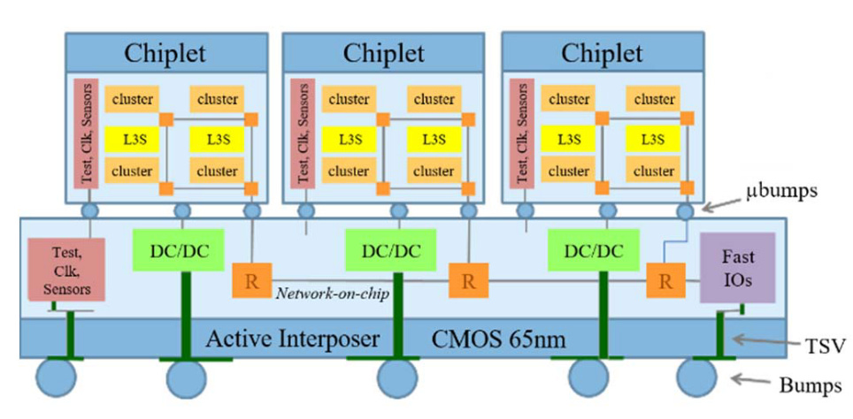
Instead of 3D-stacking two complete chips, a diluted approach is to use active interposers. These are similar to the passive silicon interposers we looked at before but have active electronics on them — implying that the front end of the chip is processed to form transistors, in addition to having RDL and TSV.
Take for example, CEA-LETI’s demonstration of the active interposer approach in 2020 ISSCC. The system consisted of 6 multi-CPU chiplets built on 28 nm fully-depleted SOI technology and stacked on top of an active interposer built on 65 nm CMOS using ultra-fine copper pillars.
The interposer includes a Network-on-Chip (NoC) which acts as a data router to provide connectivity between any two CPU chiplets. In addition, it could also include power management, I/O circuits and sensors. All this functionality is built on a mature node, leaving the CPU chiplets to be built on leading edge process nodes reducing overall cost of the system on chip.
However, there are two important considerations when using 3D stacking technology.
Thermal management: As chips are vertically stacked, it is increasingly difficult to remove heat from the base die. Extra care is required to design cooling mechanisms to maintain chips at normal operating conditions and also requires 3D aware silicon floor planning.
TSV keep-out zones: When using TSVs on active interposers, an exclusion zone between the TSV and active transistor is required to ensure that transistor performance is not affected by the TSV. This results in reduced TSV interconnect density in active interposers compared to passive ones, or higher area (TSV penalty) to support a given TSV count.
Hybrid Bonding
SemiAnalysis believes that hybrid bonding is the most transformative technology yet since the invention of EUV lithography — the next quantum leap in chip packaging since the arrival of flip-chip technology in the 90s. Here’s why I agree.
The best micro-bumping technologies have a pitch of about 5 microns, and it is getting progressively harder to make it any finer. Using hybrid bonding, researchers have already demonstrated connections with a pitch of 0.4 microns, and this is only getting started. This enables over 10 million interconnections per square millimeter — orders of magnitude higher compared to what is possible even with the best micro-bumping technology available today.
Hybrid bonding is a process used to vertically stack chips or even entire wafers without the use of any bumps or copper pillars. The stacking of one chip/wafer on another entirely relies on direct fusion of copper-to-copper and dielectric-to-dielectric; hence the name hybrid bonding, also referred to as hybrid bonding interconnect, or HBI.

The simplified process flow for hybrid bonding is as follows:
Two wafers are are surface treated to make them hydrophilic and aligned face to face. The copper pads where the interconnect will be made is slightly recessed from the oxide that surrounds it.
The wafers are contacted and the oxides form weak bonds together at room temperature.
Slowly, the temperature is increased which (1) causes the oxide to form a strong bond, (2) expands the copper pads on each wafer so that they touch.
The wafers are held at 300-400°C for a few hours till the copper pads and dielectrics fuse completely.
The bonded wafers are then diced out into 3D stacked chips.

For this to work reliably, the surfaces of each wafer must be exceptionally free of particles and have atomic level flatness. Any unwanted particles or non planarity of the oxide surfaces could result in disconnects and bulging. The depth of the copper recess is also precisely controlled: too low, and it will not expand enough to make the connection; too high, and expansion will cause the bonding interface to detach.
There are two forms in which hybrid bonding can be implemented:
Wafer to Wafer (W2W): In this method, entire wafers are hybrid bonded to each other. This requires the wafer to be extremely flat with no warpage issues. The flatness is achieved using chemical metal polishing (CMP) — a key step for W2W HBI. With this method, interconnect pitches below 0.5 microns are possible. The downside of bonding entire wafers together is yield, especially when working with advanced technology nodes. There is a high chance that the chip on the first wafer, the second wafer, or both do not work.
Die to Wafer (D2W): The chip is first diced from the wafer and then flipped and bonded to a full wafer. The benefit of this approach is there is lesser yield loss because only known good die are packaged onto the final wafer.
The interconnect pitch is not as fine as W2W, being limited to about 2 microns primarily due to alignment issues of the die to wafer among other problems like thermal expansion mismatch. There is also the issue of cleaning chip surfaces after dicing to be particle free which is much harder to do for individual chips than full wafers.

Hybrid bonding technology is still in its early days. Today, this packaging method is being used for 3D NAND flash memory and some CMOS image sensors. Hybrid bonding is useful for building future HBM technologies where there are whispers of it being used to build stacks of 16 or more DRAM chips.
We will have to wait and see how this fascinating technology unfolds.
References
SemiAnalysis Advanced Packaging Series - Part 1, 2, 3, 4, 5.
Semi Engineering: Challenges Grow For Creating Smaller Bumps For Flip Chips
Semi Engineering: Scaling Bump Pitches In Advanced Packaging
Semi Engineering: Fan-Out Panel-Level Packaging Hurdles
Semi Engineering: What’s next for TSVs
IEEE Spectrum: Hybrid Bonding Plays Starring Roles in 3D Chips
Fan-Out Wafer Level Packaging, John Lau. Springer 2018.
J. H. Lau et al., “Panel-Level Fan-Out RDL-First Packaging for Heterogeneous Integration,” IEEE Trans. Compon., Packag. Manufact. Technol., vol. 10, no. 7, pp. 1125–1137, Jul. 2020, doi: 10.1109/TCPMT.2020.2996658.
N. Islam, K. H. Tan, S. W. Yoon, and T. Chen, “High Density Ultra-Thin Organic Substrates for Advanced Flip Chip Packages,” in 2019 IEEE 69th Electronic Components and Technology Conference (ECTC), Las Vegas, NV, USA: IEEE, May 2019, pp. 325–329. doi: 10.1109/ECTC.2019.00056.
X. Wu et al., “Bump-Fabrication Technologies for Micro-LED Display: A Review,” Materials, vol. 18, no. 8, p. 1783, Apr. 2025, doi: 10.3390/ma18081783.
M. Motoyoshi, “Through-Silicon Via (TSV),” Proc. IEEE, vol. 97, no. 1, pp. 43–48, Jan. 2009, doi: 10.1109/JPROC.2008.2007462.
P.J. Tzeng, J.H. Lau, C. Zhan, Y. Hsin, P. Chang, Y. Chang, and J. Chen “Process integration of 3D Si interposer with double-sided active chip attachments,” IEEE/ECTC Proceedings, pp. 86-93, Las Vegas, NV, 28-31 May 2013.
F. Sheikh, R. Nagisetty, T. Karnik, and D. Kehlet, “2.5D and 3D Heterogeneous Integration: Emerging applications,” IEEE Solid-State Circuits Mag., vol. 13, no. 4, pp. 77–87, 2021, doi: 10.1109/MSSC.2021.3111386.
P. Coudrain et al., “Active Interposer Technology for Chiplet-Based Advanced 3D System Architectures,” in 2019 IEEE 69th Electronic Components and Technology Conference (ECTC), Las Vegas, NV, USA: IEEE, May 2019, pp. 569–578. doi: 10.1109/ECTC.2019.00092.
Detailed YouTube playlist about packaging technologies
Disclaimer: The views, thoughts, and opinions expressed in this newsletter are solely mine; they do not reflect the views or positions of my past, present or future employers or any entities I am affiliated with. The content provided is for informational purposes only and does not constitute professional or investment advice.
Thanks Vikram! Great primer, and I appreciate the references!
Good one ,helps clear the clutter,around the terminology