
While I was in the Bay Area last month attending Hot Chips, I asked Avicena if they would host me for a few hours and show me around their facility, and more specifically, show me their MicroLED technology. They graciously agreed.
I was particularly interested in seeing microLED tech first hand because there has been a lot of debate whether microLEDs are a viable interconnect technology in the datacenter. My purpose was to ask as many questions as I can, to see if I can make sense of whether standard objections to this technology hold up, and allow people actually building this technology to give their account first hand instead of simply inferring from papers, conferences, or opinions.
Most impressively, the entire top brass of the company – from their CEO, Marco Chisari, to the entire senior management of the company in charge of various parts of the business – hosted me and discussed various aspects of their technology. What follows in this report is my observations from the visit mixed in with my own research and opinions of where I think microLEDs are going.
Disclaimer: This article is not sponsored by anyone. The only ‘compensation’ was the bubbly water I drank at Avicena. Not that they did not have other stuff to offer, I just wanted bubbly water. My goal is to provide a neutral, factual account of where this technology is headed while being as informed as possible. If I got something wrong, reply to this email and let me know. This stuff is complex.
Avicena reviewed a draft of this article for factual accuracy. I retained editorial independence.
What’s in this article
Free section:
Common objections and claimed benefits of microLED interconnects: lane rates, reach, fiber count, jitter, crosstalk, gearboxing
Lane rates: where Avicena’s production microLEDs run today (3 to 3.5 Gbps), the 8 Gbps next-gen device I saw in the lab, and why there is no roadmap to catch microVCSELs on per-lane speed
Reach: why chromatic dispersion caps microLEDs at about 10 m, why the real competitor is copper and not laser optics, and what a 300+ lane cable looks like at 5 m
Paid section:
Crosstalk and jitter: victim/aggressor bathtub measurements on a live LightBundle link, with aggressors on and off, same and different PRBS patterns, and what the results say about signal integrity at 3 Gbps
Gearboxing: what 64:1 versus 4:1 ratios actually cost in chip design, clock forwarding, deskew, and whether gearboxing can be removed entirely
Physical construction and manufacturing: the transmit/receive chip, solder ball microLED integration on 300 mm wafers, molded lens arrays, fiber bundle alignment and connectors, the in-house Aixtron reactor, and the path to volume
Concluding thoughts: the 30 m reach question, redundancy and temperature behaviour, the SK Hynix scale-in request, and where microLEDs fit against copper at 1.6 Tbps
By reading this post, you agree to the terms and conditions. Also see the full ethics statement.
If you’re new, check out the About page. A lot of readers expense the subscription to this newsletter as it helps their professional work. Group subscriptions (3+) are 20% off. If you have any questions, reply to this email and let me know!
Check out the Semi Doped podcast, and our daily free newsletter with latest semi news. For institutional research, contact me at SemiExponent.
Common Objections/Benefits to MicroLED Technology for Interconnects
A framework I had while going into this, was to deliberately list out why people think MicroLEDs will not work for interconnects and try to address it during my visit. Here is a list of common objections:
Lane rates: MicroLEDs are too slow on a per-lane data rate basis and scaling to higher lane rates is hard.
Poor reach: The linewidth of microLED light is poor, and chromatic dispersion in the cable will ultimately limit its reach. 10 meters or below is believable, but 30 meter reach at good BER is a stretch.
Fiber count and alignment: A consequence of (1) is that too many fibers are required to get the lane rates to any meaningful speeds. Adding fibers is not a scalable solution. Cable itself gets bulky. Aligning hundreds of fibers to the array of microLEDs is difficult to do, especially at scale.
Jitter: MicroLEDs are very noisy, cause a lot of jitter and degrade the bit error rate (BER).
Crosstalk: Bundling 100s of fibers together means that there is a lot of crosstalk. Not too many critics clarify what they mean by crosstalk. There are two kinds: (1) between optical fibers carrying light, and (2) between different electrical lanes at the two ends of the cable that have to feed the hundreds of lanes.
Gearboxing: The SerDes on the IC side provides 8x200G lanes, for example. Converting this to say 400x4G lanes requires a gearboxing chip that is difficult to do.
The benefits stated for microLEDs are low power, low cost, better thermal performance, better availability compared to lasers, high bandwidth densities, simple silicon integration and more reliability stemming from redundant links in the array.
We’ll discuss these in detail next.
Lane Rates
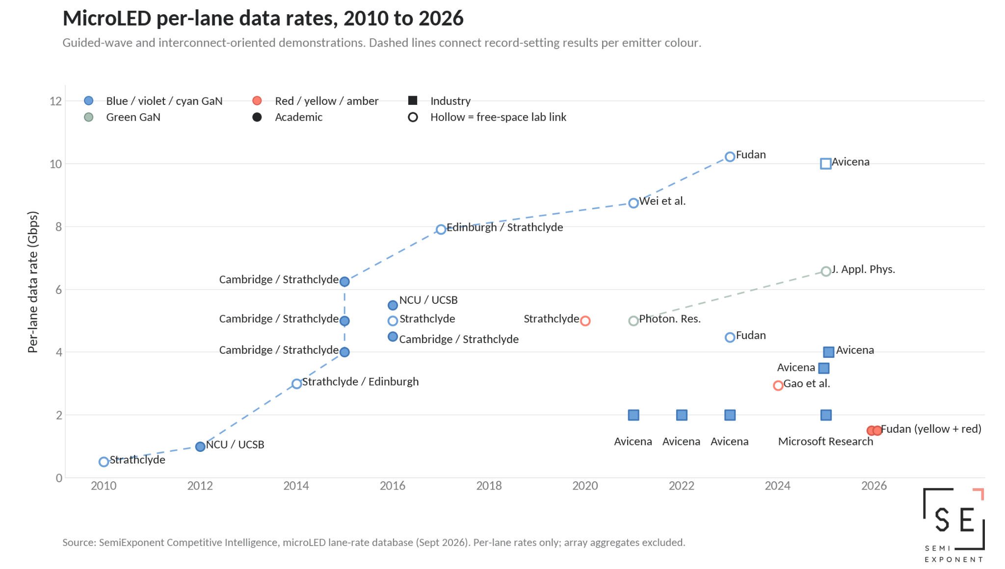
Avicena’s microLEDs are built on GaN technology, and emit blue light in the 420 to 440 nanometer wavelength range. Their current production process has a data rate of 3-3.5 Gbps per microLED. The chart below shows the evolution of data rates in microLEDs across industry and academia. These are raw lane rates only, with no consideration for reach or BER.
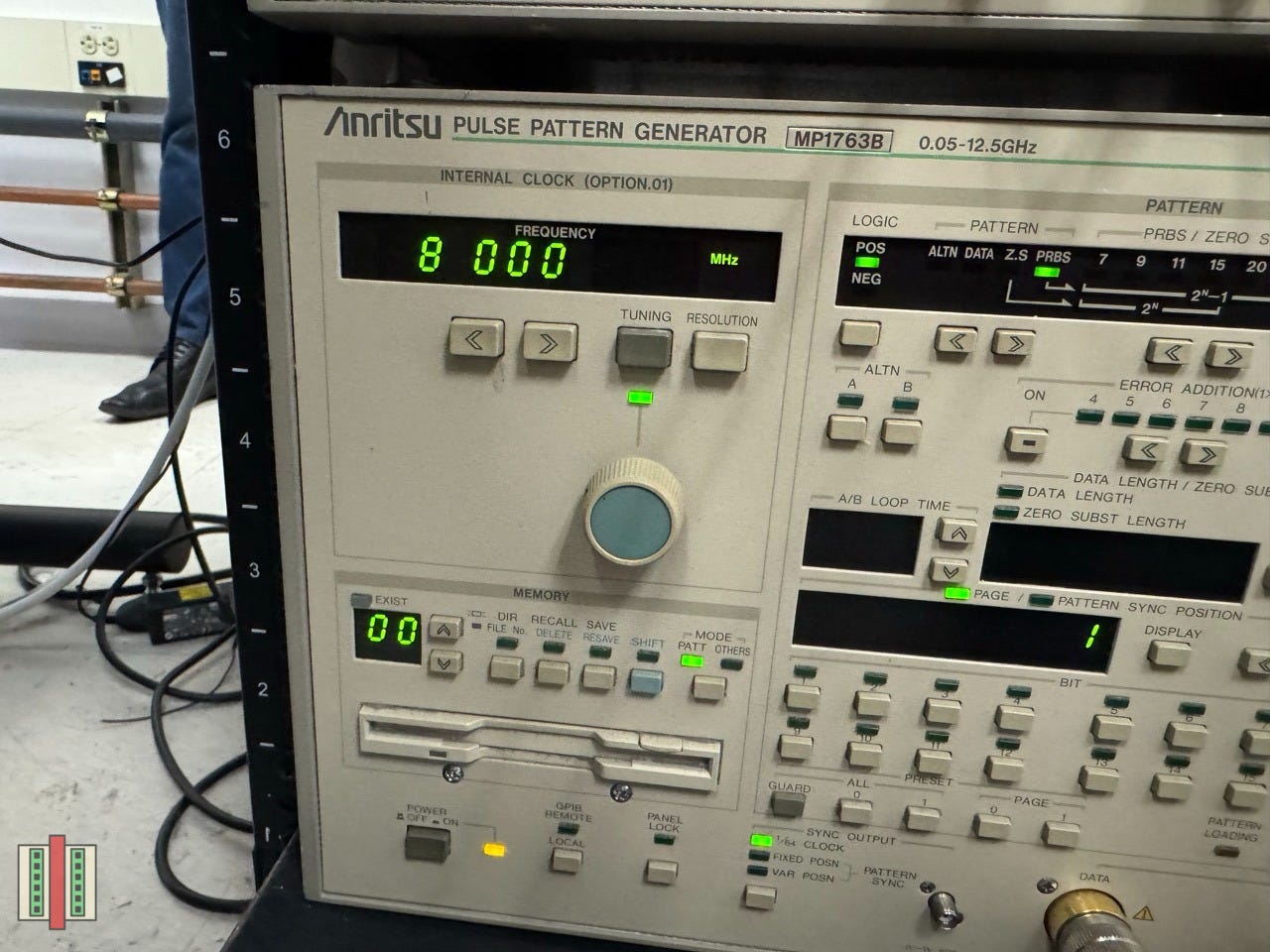
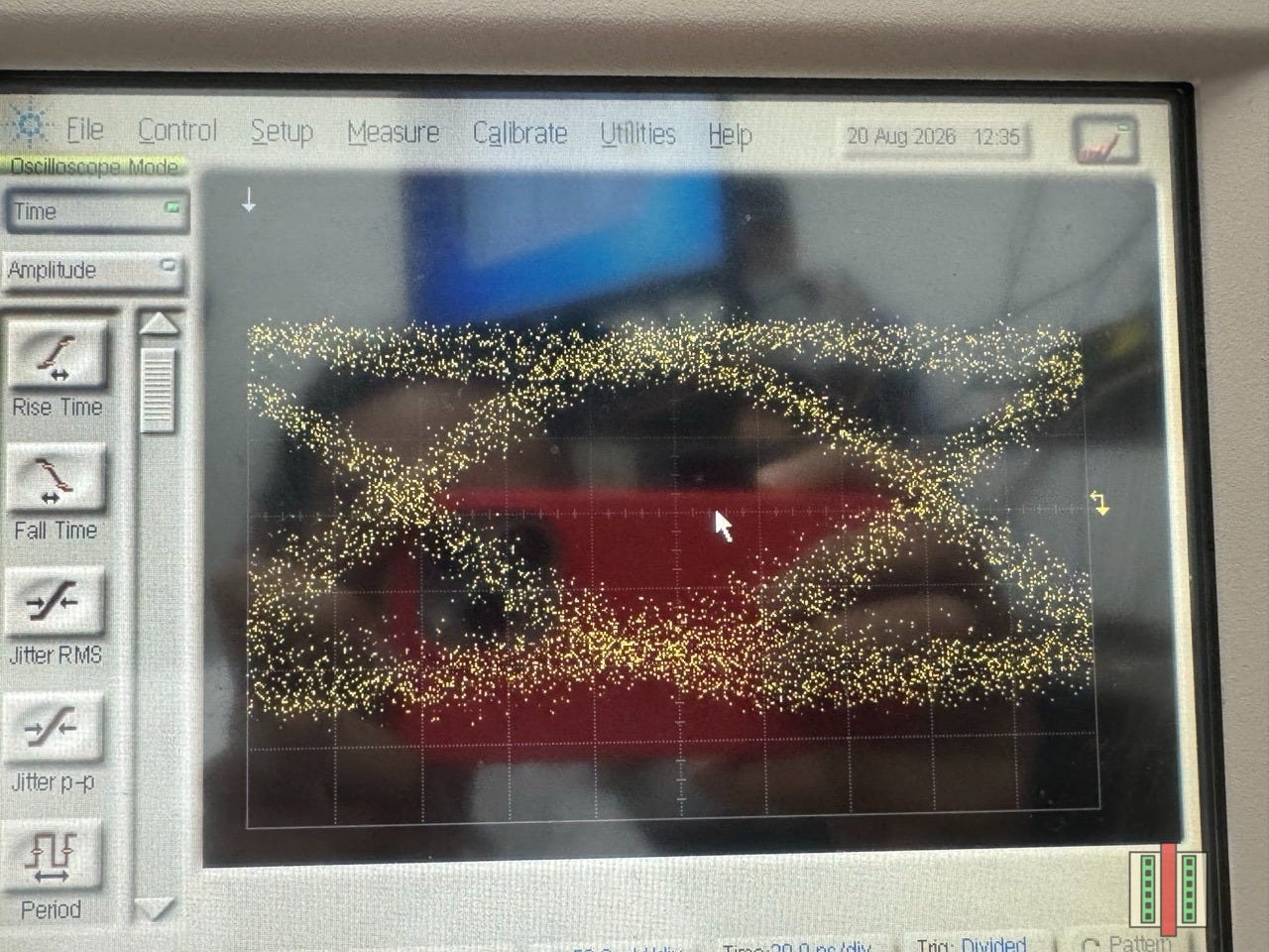
Avicena’s next gen microLEDs are still in the lab, but I got a chance to see it in action running at 8 Gbps. The important thing to understand is that this speed is not through fiber, but instead a very short free space link in a lab. Think about shining the microLED right into the detector kept a really short distance away. This approach removes the impact of the optical fiber and shows just the data rate of the microLED. Here are some pictures I took.
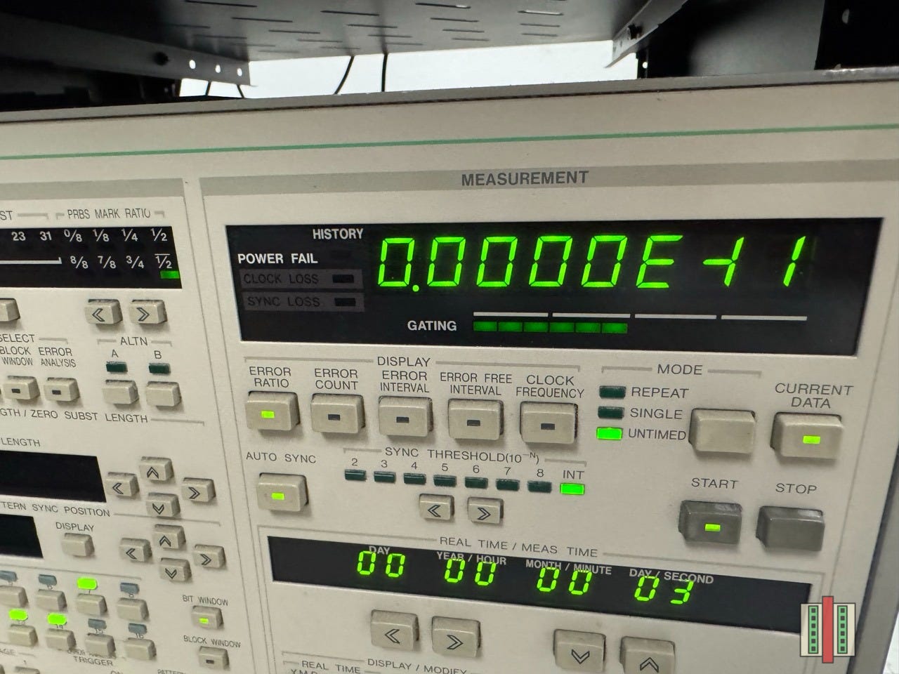
Here is the pulse pattern generator running at 8 GHz.
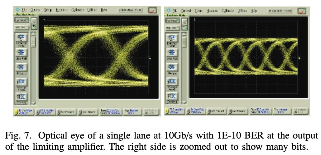
The eye-diagram from the scope runs an NRZ TX-RX short link over free space, which looks pretty clean. Jitter is quite low, and the eye is wide open.
The BER measurement shows better than 1e-11, which signifies that the eye is clean. Again, there are no channel impairments here and the results are free of chromatic dispersion which will limit reach at good BER.
In the chart above, the Avicena data point showing 10 Gbps is an interesting one (doi: 10.1109/LPT.2025.3552708). In this work, they drove the microLEDs with an external driver circuit instead of an integrated one, and were able to show bit rates of 10 Gbps per lane, with 1-e10 BER. Avicena also stated that they’re developing a next generation optical engine that will support 8 Gbps links with LEDs and PDs integrated onto a new ASIC.
The landscape of microLEDs says that lane rates will stay in the few Gbps range for a long time. There are companies who are trying to optimize microLEDs to be suited to communications; one example is Palomino Labs, who are trying to engineer the device structure to produce a narrower cone of light from a microLED. The key takeaway is that there is no roadmap to become competitive with microVCSELs (which run quite easily at 50 Gbps) on per-lane speed alone and the focus is to deliver higher bandwidth density with more lanes at smaller microLED pitch sizes.
Reach
The linewidths of microLEDs are wider than those of lasers. This wide linewidth causes light pulses launched into an optical fiber to get wider as the light pulses travel down an optical fiber. This is called chromatic dispersion and it limits the reach of the optical link because the pulses start to overlap. Pulses from a narrow linewidth light source can go much farther down a fiber before bits start to overlap each other. A wide linewidth source like MicroLEDs have bits starting to overlap in a much shorter distance. Hence, the reach of MicroLEDs is inherently limited.
We’ve discussed this in quite some detail in the free article below if you need more background.

Too many people equate microLED interconnects to optics for scale-out applications where the reach is over 10m. This is partly a problem with companies developing this tech too, because they advertise 30-50m reach which draws comparison to laser-based optics. This is the wrong way to think about it and I wish companies would stop overpromising on technology that has not demoed on a showfloor yet.
The real high-value use cases for microLED interconnects today cover reaches up to 10m, until somebody shows solid technical measurements to prove otherwise (Credo at OCP: I will be there, bring your wares). The real competition is copper, not optics, as shown below.
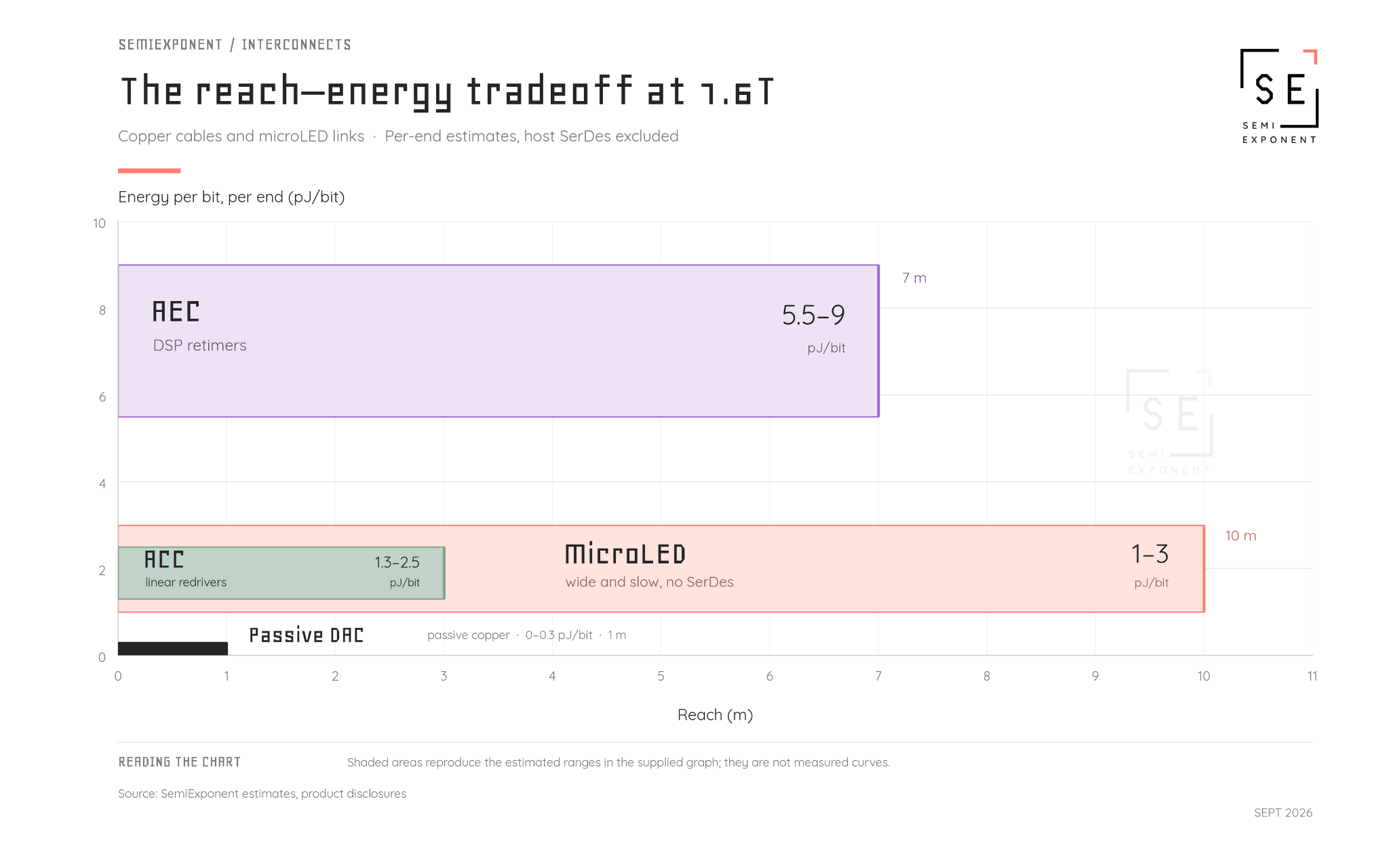
The reach of an active electrical cable (max 10m), at the power consumption of a DSP-less active copper cable (1-3 pJ/bit).
It is clear how microLED occupies an important and attractive tier in the close-reach interconnect space. Especially as the scale-up domain is going multi-rack in the Rubin Ultra and beyond, MicroLEDs provide a solution to connect GPUs both in-rack and across-racks, at an energy-efficiency that is attractive as world-sizes go up.
The setup below shows Avicena’s LightBundle™ which they sample to potential customers along with their software platform shown on their screens. The boxes have transmit and receive circuits, and are used to test the microLED link between them. They have internal waveform generators if you want to use data patterns out of the box, or the front panel has connectors through which customers can provide their own waveforms for testing the optical link.
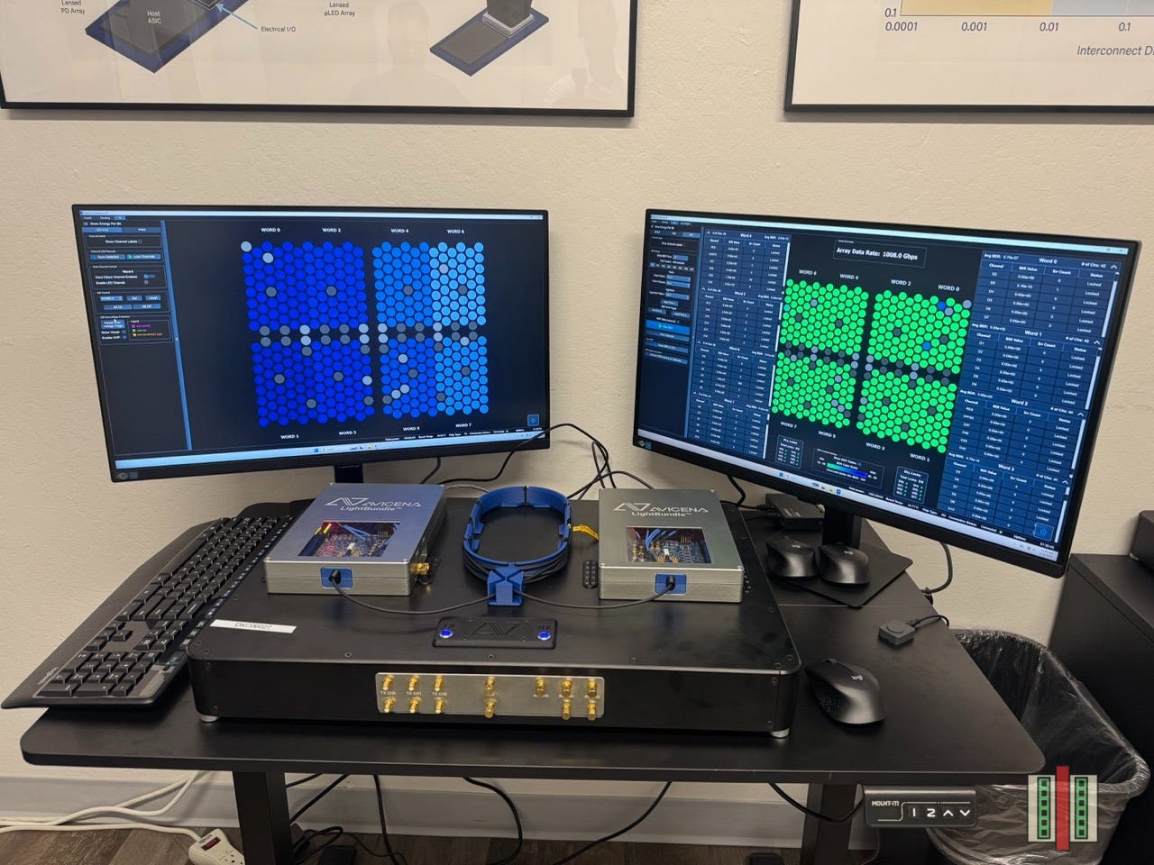
The length of the cable in the middle is approximately 5m in this test, and the diameter of the cable having 300+ parallel links is 3mm. The idea that a bundle of fibers makes the actual cable unwieldy is untrue.
The screens show transmitter data on the left, and receiver data on the right. Each of those hexagons on the screen represent a microLED lane carrying ~3 Gbps of data. You notice there are some blue dots on the grid – those are the points where the link is performing poorly, where the BER is higher than some threshold. The bottom of the screen shows a color scale from green to blue: green = good BER, blue = bad BER. We will see some measurements with this setup next.