
An In-Depth Look at the Viability of X-rays as an Alternative to EUV Lithography
Substrate - a California startup wants to take down both TSMC and ASML using X-rays to pattern leading edge nodes below 2nm. But how viable is their technology?

Welcome to a 🔒 subscriber-only deep-dive edition 🔒 of my weekly newsletter. Each week, I help investors, professionals and students stay up-to-date on complex topics, and navigate the semiconductor industry.
If you’re new, start here. See here for all the benefits of upgrading your subscription tier!
As a paid subscriber, you also have access to a video explanation of this post, an executive summary with key highlights, and a google drive link to this article so that you can parse it with your favorite LLM to mine insights best suited to your needs.

On October 28th 2025, Substrate emerged from stealth with $100M in funding and a $1B valuation. The California startup has demonstrated proof-of-concept lithography tools competitive with ASML and fabs like TSMC, Intel and Samsung capable of leading edge nodes at potentially a fraction of the cost. The specific interest centers on X-ray lithography (XRL) as a successor to extreme ultraviolet (EUV) lithography used in today’s leading chip technologies.
This matters because TSMC, Samsung, and hopefully Intel, are the only foundries capable of mass-producing chips at the leading edge and ASML is the sole provider of lithography tools capable of producing these advanced nodes. Already, most American major fabless companies heavily rely on TSMC to manufacture their chips. Substrate’s technology might change all that. America once led chip manufacturing but ceded that position to Taiwan over decades of policy decisions. Substrate’s success means that America “will lead again” in chip manufacturing — if the technology actually pans out at scale.
To be clear, I actually have no idea if this will work, if Substrate’s claims are actually true, or how skeptical one has to be. Take any drastic claims with a healthy grain of salt, because, as Substrate’s CEO James Proud has said himself, this is an incredibly difficult problem but an extremely important one.
This article is intended to provide a better understanding of XRL as a logical successor to EUV. To provide context, we will start with the basics of lithography and trace its evolution so that the need for XRL is clear. Then, we will discuss the challenges and benefits of XRL, and conclude with some thoughts on Substrate.
Here is an outline:
Photolithography and optical masks
Wavelength and Aperture for photolithography
EUV lithography
X-ray lithography and Substrate
X-ray sources
Challenges in X-ray optics
Challenges in X-ray masks
X-ray lithography’s potential throughput advantage
For paid subscribers, I provide my thoughts about the future of Substrate and X-ray lithography.
Reading time: 18-20 mins
Photolithography and Optical Masks
Lithography is the process of patterning tiny geometries on a silicon wafer that enables us to create modern-day transistors used in leading edge nodes. The simplest way to think of the lithography process is to think of developing film cameras. In order to pattern shapes on a silicon wafer, much like a picture on a photograph, a negative called a mask is required to allow light to pass through in some areas while blocking it in others. By selectively blocking parts of the silicon wafer, the exposed parts are cured in the presence of light, while unexposed parts can be washed away, leaving the underlying pattern exposed. Initially, these photolithography masks were cut with an exacto knife based on a chip layout drawn on graph paper. But as you can imagine, this process does not scale very well with smaller dimensions.
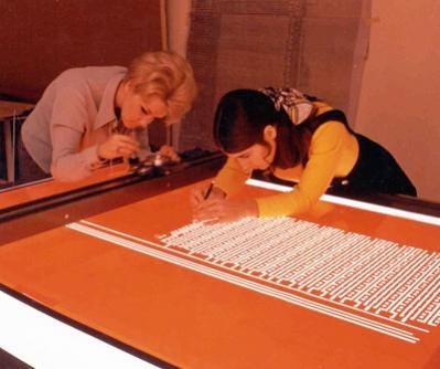
Jay Lathrop along with colleague James Nall in had a brilliant idea in the late 50s to solve the problem while working at the Diamond Ordnance Fuze Lab (DOFL) trying to miniaturize electronics for proximity fuses. They took a microscope and turned it upside down so that instead of magnification, it results in smaller features. Using the same idea, they shone light through an inverted microscope which resulted in smaller patterns being imprinted on the silicon mask. This was the cornerstone of modern lithography.
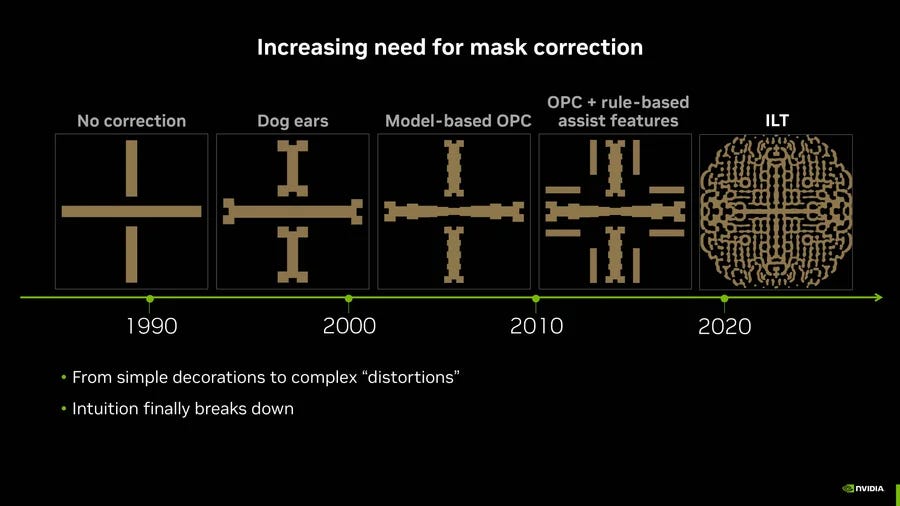
Today, the masks are much much more complicated due to the way light diffracts and bends at nanometer scale wavelengths. For a leading-edge process like TSMC 5nm requires as many as 81 masks with an approximate cost of $100K USD per mask. They are designed in extremely complicated machine learning-assisted ways using a process called inverse photolithography, which, interestingly, uses Nvidia GPUs for its creation. Asianometry has a series of videos on semiconductor masks, computational lithography, and most recently, on curvy masks; you should binge many related videos on the channel.
Regardless of the mask patterning technique, two major factors that control feature sizes are light wavelength and numerical aperture of the lens system.
Wavelength and Aperture for Photolithography
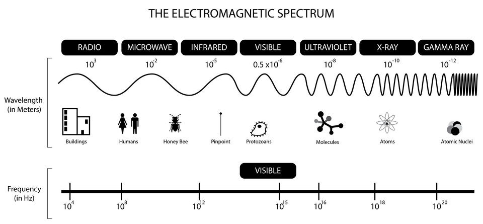
The early light sources that Jay Lathrop used to miniaturize integrated circuits were broad-spectrum mercury vapor lamps that had a wide range of wavelengths, which were then filtered with near-ultraviolet (UV) light filters. They were mostly in the range of 365-436nm wavelengths. As transistor sizes scaled down, it became important to control the wavelength of light used to expose photolithography masks and is determined by the Raleigh criterion:
Here, CD means the smallest feature size that is possible using the lithography system. k1 is a proportionality factor that encapsulates techniques like optical process correction (OPC) that have been used to make finer feature sizes (we won’t discuss this here). The two other significant factors that control minimum feature sizes are:
The wavelength of light being used (lambda): This is essentially the color of light being used. The more it is towards the ultraviolet spectrum, the smaller the wavelength and smaller the feature sizes that are possible.
The numerical aperture of the lens system (NA): This is a measure of the total range of angles over which a lens can collect light. When light emerges from the photolithography mask, it is diffracted and a high NA lens will be able to capture most of the diffracted light, which allows smaller dimensions to be featured on the wafer. Much like photography lenses, a high numerical aperture lens requires high refractive index materials, and can collect a lot of light with a shallow depth of focus. This implies higher focus control and flatter wafers are needed.
In the 1990s, photolithography processes to manufacture 130-250nm nodes used a Krypton-Fluoride (KrF) excimer laser that generated a light wavelength of 248nm in the deep ultraviolet (DUV) region. Soon this gave way in the 2000s to an argon fluoride (ArF) excimer laser with 193 nm wavelength, which was the mainstay for 45-90 nm nodes. Wavelengths still needed to go shorter if transistor sizes had to go below the 45 nanometer node. Sadly, physics hit hard limits.
For a brief time, a 157 nm fluoride laser was considered, but faced challenges: it was strongly absorbed by oxygen and water vapor and required vacuum optics, traditional fused silica optics were opaque to this wavelength, and new photoresist materials suitable to 157nm was required. Shorter wavelength argon lasers at 126 nm also posed similar challenges. So the only way was to increase numerical aperture instead.
Luckily, the solution was silly, simple and elegant: add water. The 193nm ArF laser is passed through a layer of ultrapure water between the final lens element and the silicon wafer, giving it the name immersion ArF (ArFi) lithography. Compared to “dry” lithography techniques used earlier, water’s refractive index of 1.3-1.4 increased the NA, and allowed the CD to reduce by 30-40%. This allowed the process nodes to scale down to 20 nm in the early 2010s.
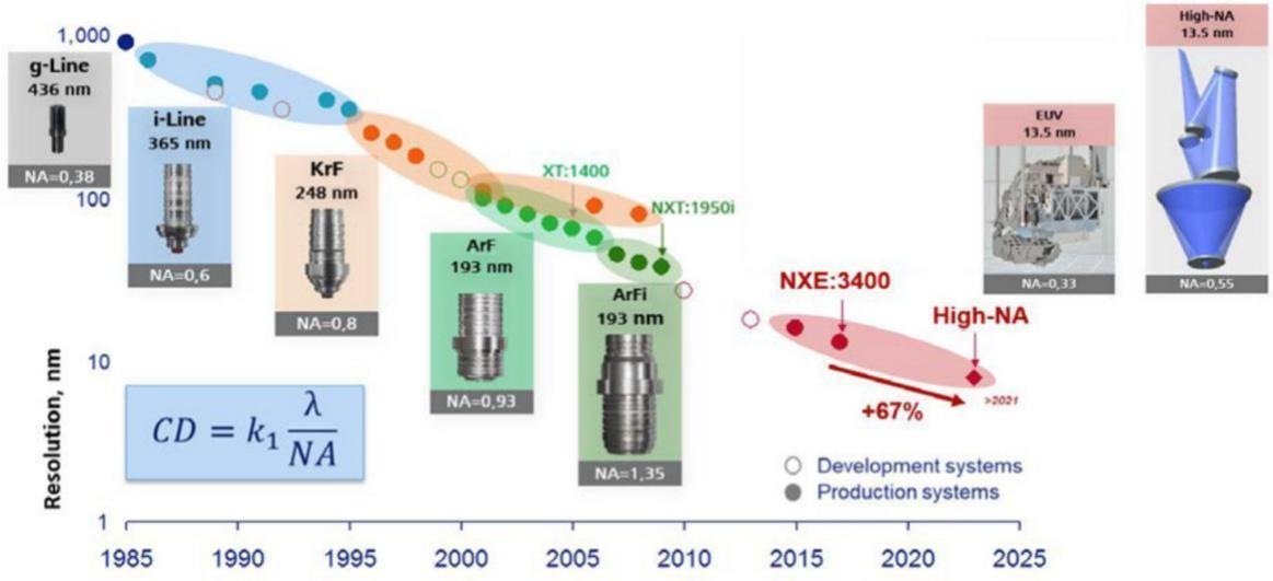
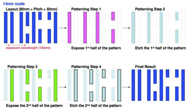
The next question was how to go even smaller - down to 10nm nodes. Wavelength and numerical aperture already hit their limits with DUV, so during the mid-to-late 2010s, transistor scaling continued because of the use of double patterning. The idea is simple: Take a fine-pitched patterning pattern and split it into two coarser patterns. Pattern each one on the wafer individually using litho-etch-littho-etch - often called LELE. The principle could be extended to triple (LELELE) or even quadruple patterning. There are more tricks to push the capabilities of ArFi DUV, but we’ll move on to EUV.
At this point, it should be noted that it was at this 10nm crossroad that Intel famously chose to take the safe path with ArFi DUV that arguably resulted in them falling behind on leading edge lithography because they chose to not be an early adopter of the highly expensive next generation lithography technique, extreme ultraviolet lithography (EUV).
Extreme Ultraviolet (EUV) lithography
EUV was a technology that was decades in the making, with the brightest American minds working in the nation’s top research labs. The development process required millions of dollars of funding from various companies, including Intel, who invested $200 million in its development but would later hesitate to adopt it. Silicon Valley Group was the company best positioned in the late 90s to commercialize EUV technology. At the time, it was the only US company building high-end steppers and scanners, competing with Nikon and Canon. In 2001, Silicon Valley Group faced cost overruns, weak cash flow compared to its competitors and limited ability to fund EUV R&D. It was then sold to ASML. The US government approved the sale. The future of American chip manufacturing was lost forever.
EUV uses a dramatically different way to generate light. It blasts tiny droplets of tin moving at several hundred miles per hour with a high-powered carbon-dioxide laser. The first laser pulse heats up the tin droplet, and the second pulse blasts it into a plasma with a temperature around half a million degrees. This process is repeated 50,000 times per second to generate light at 13.5 nm which is a significant reduction in wavelength from 193 nm ArF, and paved the way for advanced logic nodes below 10 nm.
While the mechanism of creating EUV light is itself incredibly complex, the optics associated with it are even more so. EUV wavelengths are much closer to X-rays, which makes them hard to reflect without special mirrors made up of 40-50 alternating layers of ultra-thin molybdenum and silicon and a mind-bogglingly smooth surface, which is quite possible among the most precise manufacturing humans have ever achieved. In Chip War, Chris Miller writes:
If the mirrors in the EUV system were scaled to the size of Germany, … , their biggest irregularities would be a tenth of a millimeter.
Today, a single EUV machine costs a quarter of a billion dollars and is only manufactured and sold by ASML. The incredible cost and complexity of the machine puts it out of economic feasibility for a lot of major chip manufacturers in the world.
In 2018, a medium sized foundry like GlobalFoundries decided to abandon pursuing 7nm nodes and below even after spending $1.5 billion on the EUV program. By the end of 2020, only TSMC and Samsung had enough history with EUV lithography to continue pushing to smaller nodes. Intel’s late EUV start pushed them back, and led Pat Gelsinger to try and “catch up” by advancing 5 nodes in 4 years (5N4Y). Intel would eventually skip several nodes in between, although the race to 2nm and below is still firmly on.
At 2nm, low-NA is currently state-of-the-art in production. Low-EUV can produce tight metal spacings without the need for multipatterning, but as we continue to scale down, multipatterning becomes an inevitability and adds undesirable complexity. In 2026, ASML’s newest high-NA EUV lithography tool, the EXE:5000, is slated to start production at an estimated sticker price of half a billion dollars.
SemiAnalysis has expressed healthy skepticism whether high-NA single patterning will be more cost effective compared to low-NA multipatterning. ASML’s planned next-gen lithography tool - hyper-NA EUV - is just pointlessly expensive. At an estimated cost of a billion dollars for just the lithography tool, it probably does not make economic sense to make these chips anymore.
Unless … we can again go to smaller wavelengths like we did when we went from DUV to EUV.
Enter XRL and Substrate, the startup we mentioned at the beginning.
X-Ray Lithography (XRL) and Substrate
XRL is not a new idea but it allows the use of wavelengths from 0.1-10nm for lithography, which opens doors to reducing CD even further. It was first proposed by H. Smith and Spears at MIT, with the first patent publication in 1973. Throughout the 1980s, IBM put in substantial resources behind building XRL manufacturing facilities all over the United States, which they demonstrated by fabricating high-resolution DRAM devices. Motorola even joined in on IBM’s effort.
By the mid-90s, the effort on XRL largely dissipated because it required a broad collaboration between a number of companies and they couldn’t come to terms on how the intellectual property generated from the collaborative effort would eventually be distributed. Also, the industry preferred to march down the track of UV lithography. In a 2016 review paper X-ray lithography: Some history, current status and future prospects (🔒), the authors write:
We could argue that had we persisted in our attempts to field an XRL chip technology, lithography would be cheaper, as all the optical “fixes” needed to achieve, say, a 32 nm product would be unnecessary. But given the experience with EUV lithography, new un- foreseen difficulties could arise, increasing cost and delaying time-to-insert. The only thing that can be said is that in the lithography arena, evolution has won out over revolution. It was “easier” to evolve systems, to make a series of incremental (albeit expensive) changes, rather than go to more radically different approaches.
Although there is a tinge of disappointment in the authors’ tone, XRL poses many challenges that we will discuss shortly. But perhaps it is time to face the problem head on and adopt a radical new approach instead of pushing EUV beyond its logical (and economic) limits. This is exactly a California startup has set out to do.
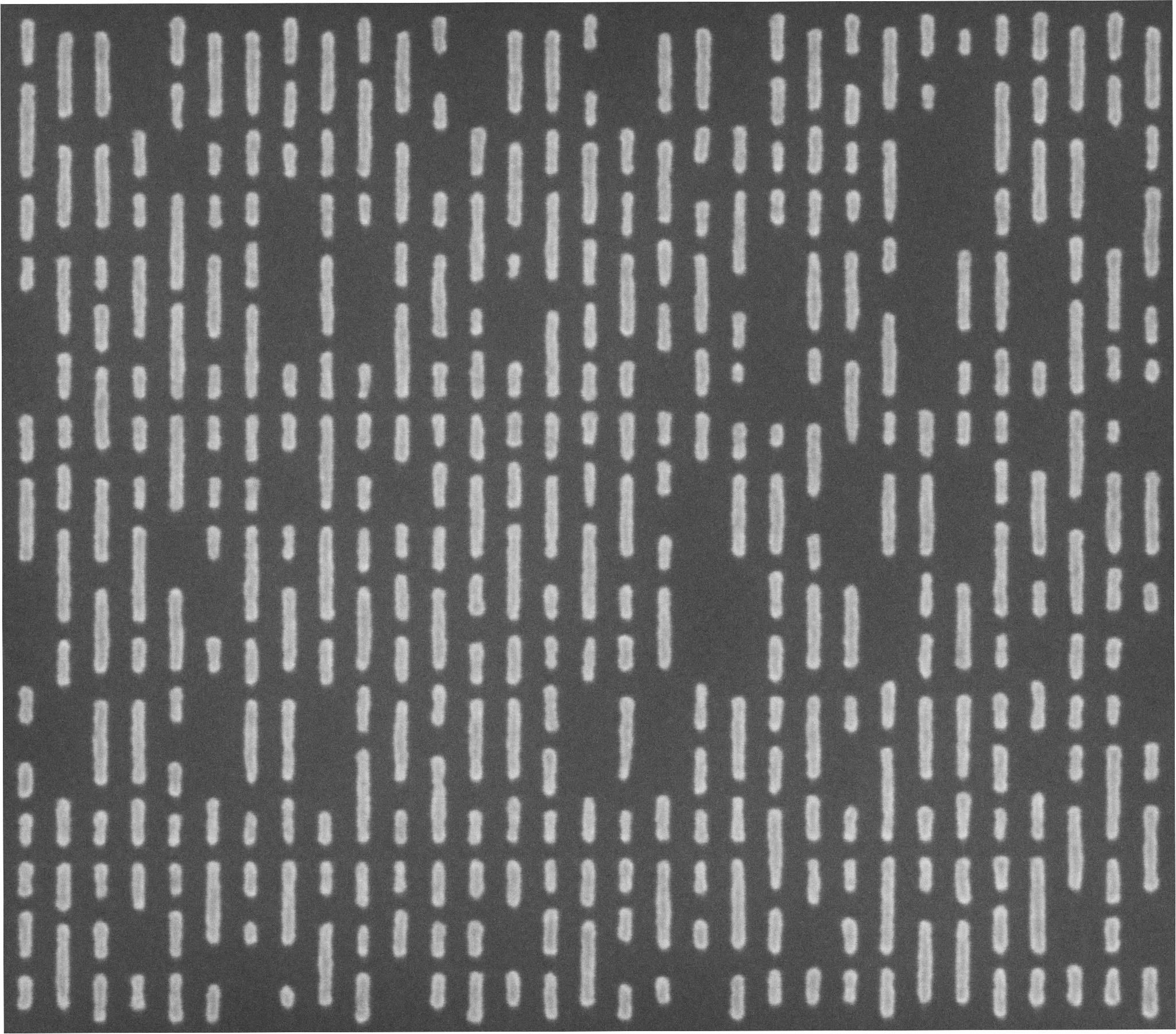
Substrate is a US-based startup that is reviving interest in XRL as UV-based approaches are nearing their practical limits. Their focus is on commercializing decades of XRL R&D performed in U.S. government research labs over the past half century. They recently released images that show fine-featured structures representative of a 2nm process node, which has been widely circulated on the internet by now. The CD between the various shapes shown here is about 12-13nm. Although my untrained litho eye sees some abnormal shapes, lithos_graphien makes some closer expert observations on X.
While this is a commendable achievement, Substrate has provided no additional information on the cost and size of sources for X-ray radiation, what optics they did or did not use, how the masks were prepared, or if throughput is comparable to EUV on 300mm wafers. In the next few sections, we will discuss these aspects.
X-Ray Sources
While blasting tin droplets with lasers generates EUV light, it is important to understand where X-rays for lithography come from.
Substrate has stated that they use particle accelerators for XRL. Its principle of operation relies on the acceleration of electrons by driving them through a series of RF cavity resonators that accelerate them. As they are accelerated, giant magnets bend the electron beam so that they can be confined to a circle, and repeatedly accelerated to high energy levels. Such a particle accelerator is called a synchrotron.
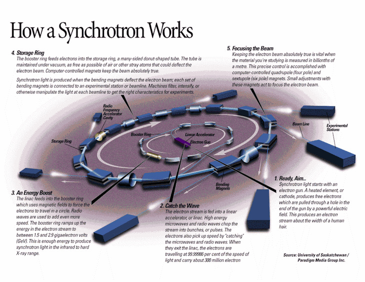
The act of forcing a charged particle to bend while moving at relativistic speeds causes it to radiate electromagnetic energy. If the energy levels are just right, it can generate copious amounts of energy called synchrotron radiation, which are in the X-ray spectrum. Such X-ray sources are often called storage rings and have been around for several decades now and are considered established and mature technology.
Synchrotrons produce some of the brightest X-ray beams available and have been used for specialized X-ray lithography applications like LIGA, especially for making higher aspect ratio microstructures for MEMS. Storage ring synchrotrons can have a circumference anywhere between 30 meters to >1 km depending on the wavelength and output power needed, and can be extremely expensive to build. But there have been continuous efforts to reduce the size of particle accelerators to table-top form factors, and even on-chip! We currently have no information on the type of X-ray source Substrate is using for chip lithography, but a literature search shows that there are a variety of options depending on what wavelength and output power is required.

Challenges in Optics for XRL
Unlike UV, X-rays are absorbed by nearly all materials, which makes it challenging to design mirrors to reflect X-rays. Mirrors have been developed for X-rays, but their principle is quite different from regular mirrors. They utilize a concept called grazing incidence optics, where X-rays reflect off mirrors at shallow angles, much like a stone thrown into water at a shallow angle skips across the surface of the water. This is how space telescopes capture and focus X-rays from outer space. Substrate has mentioned that they use some form of “optics” but it is not clear that it is grazing incidence optics.
Because conventional optics is difficult with X-rays, a different approach is required called proximity printing. Here the mask used to pattern shapes on the wafer is placed very close to the wafer (10s of microns away) and it is illuminated with X-rays. The mask casts a shadow which exposes the resist on the wafer. The fundamental limitation of this method is that feature sizes have a 1:1 printing ratio, which means that the pattern on the mask is the same size as what you want on the wafer.

Remember how Jay Lathrop flipped the microscope upside down? The advantage of using UV lithography is that you can have a mask that is larger in size than the feature being printed, usually by a ratio of 4:1 (high-NA EUV uses 8:1). This is called reductive projection optics and is a big advantage for EUV systems. Proximity printing in XRL does not provide this option, which makes masks considerably difficult to create due to the accuracy of features required.
There is another technique that is used in XRL called interference lithography only worth a mention for the sake of completeness. This involves two sources of x-rays which are used to create interference patterns and can produce feature sizes smaller than the wavelengths being used. However, because interference patterns are involved, this method can only create regular periodic patterns. It is not useful for making integrated circuits where you have to make arbitrary shapes like transistors, wires, and contacts.
Challenges in Masks for XRL
1:1 proximity printing already makes the feature sizes on the mask difficult to pattern, but the challenges go beyond that. The mask needs to be built on a material that allows x-rays to go through it while simultaneously blocking x-rays depending on the mask pattern.
XRL masks are typically built on very thin membranes made of silicon carbide or silicon nitride that are just a few micrometers thick to allow x-rays to pass through. On top of this very thin membrane, the mask is patterned using reasonably thick absorber materials like gold or tungsten to block x-rays from the wafer below. These mechanically fragile masks essentially need to be suspended over the wafer for proximity printing. Even slight distortions or warpage in the mask affects the patterned shapes on the wafer because the shapes are 1:1 on the mask.
Finally, identification of areas for mask repair for XRL is difficult because they must be inspected with X-rays. After identification, fixing the absorber materials by filling in holes, or removing excess material is difficult because the aspect ratio is very high - the resist is in the order of micrometers of thickness to effectively absorb x-rays, while feature spacing on the mask will be in the 10s of nanometers due to 1:1 proximity printing. In case of structural damage to the fragile mask substrate, the entire mask has to be discarded, which makes it very expensive.
XRL’s Potential Throughput Advantage
In spite of the disadvantages of proximity printing, the use of minimal mirror systems (with grazing incidence optics) is a distinct advantage for XRL. An EUV system uses a dozen mirrors to focus the light and 25-30% of the energy is lost at each reflection. Only about 3-5% of the generated EUV power is delivered to the wafer.
XRL’s lack of mirrors means that almost all of the synchrotron light is available at the wafer. For the same source power, XRL provides dramatically more light to the wafer resulting in faster exposure times and higher throughput. EUV systems also have to cool the heat generated in the mirrors which XRL does not have to do, which is another speed advantage for XRL. However, all of these speed advantages are lost if the fragile mask breaks and needs to be replaced.
After the paywall, I’ll provide my thoughts about the future of Substrate and XRL.