
Battle for Advanced Packaging: TSMC Monopoly, Intel Challenge, and Amkor Arms-Dealing
Intel’s advanced packaging business is now a credible source of supply for the AI accelerator industry, while TSMC keeps ramping. Amkor plays both sides.

Advanced packaging has been a one-horse race. Every leading-edge AI accelerator worth talking about gets its logic married to HBM on TSMC’s CoWoS, and for three years TSMC has had that socket entirely to itself.
According to a recent TrendForce estimate, the industry’s CoWoS capacity could reach 200k wafers-per-month (wpm), with TSMC running ~120k wpm by the end of 2026, while ASE and Amkor get a seat at the table only as overflow, soaking up something like ~80k wpm. TSMC has been rapidly building out capacity to support CoWoS demand. Most of the big GPU chips are packaged by TSMC, while simpler flows like Vera CPUs and automotive parts overflow to Amkor/ASE facilities.
Intel’s EMIB is the first credible second source to show up with real orders behind it. AWS and Cisco are already shipping external silicon on EMIB. SpaceX and Tesla signed on around the Q1 2026 earnings call as partners in Intel’s Terafab project. Google’s TPU v8e is reported to land on EMIB in the second half of 2027, with Apple, Microsoft, and NVIDIA sitting in the talks pile. CFO David Zinsner moved Intel’s external advanced-packaging outlook from a few hundred million to north of a billion dollars across the last two calls, and told CNBC he expects billions of dollars per customer. For a business that small, packaging alone going past a billion is a step change.
However, as orders flow to Intel, TSMC is continuously expanding CoWoS capacity. The increasing sizes of advanced packages for AI accelerators puts the two competitors at a crossroads again -- and this time the outcome will be decided based on what happens in the next few years as the industry moves to adopt glass core substrates.
Contents:
EMIB Comes for the CoWoS Monopoly — the three-year packaging monopoly, and the orders that are breaking it.
Deeply Understanding CoWoS-L vs EMIB — the three CoWoS flavors, and how Intel’s bridge differs from TSMC’s.
Where the Size Limitations Lie — the round-wafer-versus-panel math that caps CoWoS-L and frees EMIB.
The Convergence on Glass Core Panels — why warpage and CTE force both foundries onto glass.
Where This Leaves Investors — the winners and losers, and the OSATs that win either way.
The Taiwanese Glass Partner Already Inside TSMC’s CoPoS — the name the glass maps miss.
By reading this post, you agree to the terms and conditions. Also see the full ethics statement.
If you are not a paid subscriber, you can purchase just this article using the button below. You can find the whole catalog of articles for purchase at this link.
If you would like to engage boutique research services for your project, reach out to us.
Deeply Understanding CoWoS-L vs EMIB
Many comparisons online of CoWoS to EMIB are not precise about the exact flavors of each technology, and opens doors to misinterpretation. We’ll clarify that aspect first.
CoWoS-S is the original, a single monolithic silicon interposer. It gets really large and expensive beyond a certain size. TSMC’s limit is about 3.3x reticle size (or 2,380 mm2).
CoWoS-R swaps that silicon interposer for a cheaper organic RDL one, which is what AWS uses for Trainium 2/3 chips. They do not have the interconnect density of silicon interposers, and are rather limited in size too.
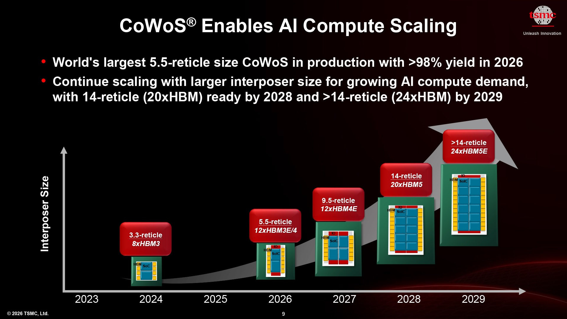
The variant carrying the biggest AI packages today, the Blackwells and the Rubins, is CoWoS-L, which scales to 5.5x reticle size (or 4,720 mm2) today, with plans to expand to 9.5x reticle size (or 8,150 mm2) in 2027. TSMC’s roadmap extends to 14x reticle size (or 12,000 mm2) by 2029.
Both TSMC’s CoWoS-L and Intel’s EMIB are built on the same idea of giving up a full silicon interposer for silicon bridges only where you need fine pitch wiring, such as die-to-die and die-to-HBM, and use cheaper routing for everything else.
TSMC calls its bridge an LSI (local silicon interconnect, and hence the ‘L’) and embeds it in an Re-Distribution Layer (RDL) interposer.
Intel calls its bridge EMIB (embedded multi-die interconnect bridge) and embeds it straight into the organic package substrate.
Note the difference in where the bridges live. CoWoS-L’s RDL interposer is built on a wafer, so it stays bound to the 300mm wafer and the reticle limit (the whole reason CoPoS and glass panels are coming). EMIB embeds its bridges in the organic substrate with no wafer carrier, so it clears the wafer-size wall, and scales to bigger interposers due to the use of rectangular panels.
Here is Intel’s EMIB roadmap in terms of size.
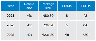
Today, Intel’s EMIB holds a size advantage by being able to deliver on 8x reticle size (or 6,860 mm2), which is ahead of TSMC’s 5.5x capability, due to the choice of rectangular formats for organic substrates rather than RDL interposers on round wafers. Intel promises 12x by 2028 as opposed to TSMC’s 14x, but we’ll have to wait and see who actually delivers, and at what reticle-size multiple.
Meanwhile, we can try and guess.
Where the Size Limitations Lie
CoWoS-L runs into a size ceiling that comes straight from the round wafer it is built on. The LSI bridges are embedded into RDL, but the RDL itself is fabricated on a 300mm silicon wafer and then mounted on an organic package substrate. While the bridges themselves are small, the RDL interposer carrying them is one big rectangle, and a round wafer yields only a few per wafer.
Let’s actually calculate who is capable of delivering a 14x reticle by 2028. On the left is a 300mm round wafer with a total area of 70,600 mm^2, representative of TSMC’s process. On the right is a 310mm x 310mm organic panel, with a total area of 96,100 mm^2, representative of Intel’s EMIB.
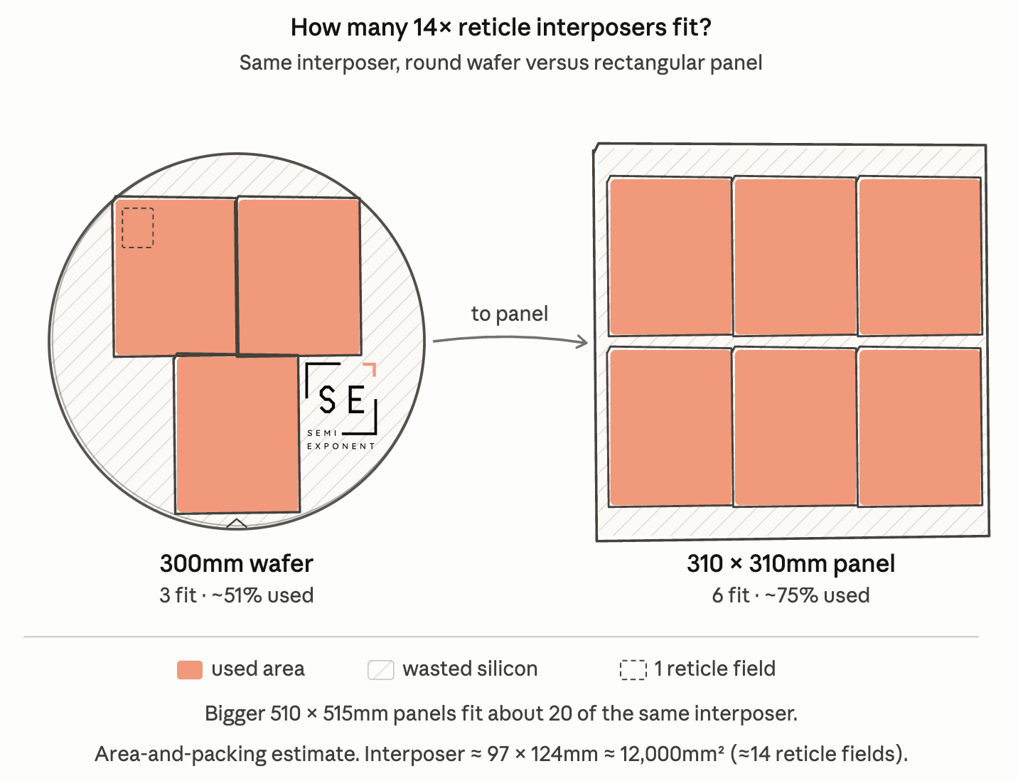
The rough excalidraw picture above shows that a round wafer fits just about three 14x-sized packages, while the rectangular panel provides six. The area utilization goes from ~50% to ~75%. A transition to bigger 510mm x 515mm panels in the future will yield ~20 interposers.
It is clear that EMIB’s use of rectangular panels is vastly superior when it comes to large package sizes. It is the same round-versus-rectangular problem pushing TSMC toward CoPoS, except EMIB already uses the rectangular format. Intel is starting where TSMC is trying to get to. What keeps TSMC ahead in practice is volume, since it ships these packages today. Intel’s advanced packaging story is just getting started, but it holds a structural advantage in large packages in the future.
The Convergence on Glass Core Panels
Unfortunately for Intel, at 14x reticle sizes, it is not just the advantage of rectangular vs round formats that matter. For such large packages, organic substrates inherently become poor candidates due to their tendency to warp, and the co-efficient of thermal expansion (CTE) mismatch with silicon. Regardless of the format, the physical properties of the material starts causing yield issues which strips away some of Intel’s lead in large size packages, and instead levels the playing field with TSMC.
The answer for both foundries is the same: large rectangular panels on glass core substrates. It has unique properties that make well suited as a core material:
It has a high degree of flatness
It has a CTE that is closer to silicon than organic materials
It has low dielectric loss (good for interconnect)
It has a high Young’s Modulus, which means that it is very stiff and needs a high degree of force to stretch it even a little.
In glass, through glass vias (TGVs) can be made much closer, which results in better power delivery due to lower parasitics.
Light propagates through glass, which opens the doors to optical integration in the future.
Intel is the first mover on glass substrates, demonstrating a 78mm x 77mm, which is equivalent to 7x reticle size. This houses 2 full reticle-sized GPUs, for example, with room for interconnections with EMIB.
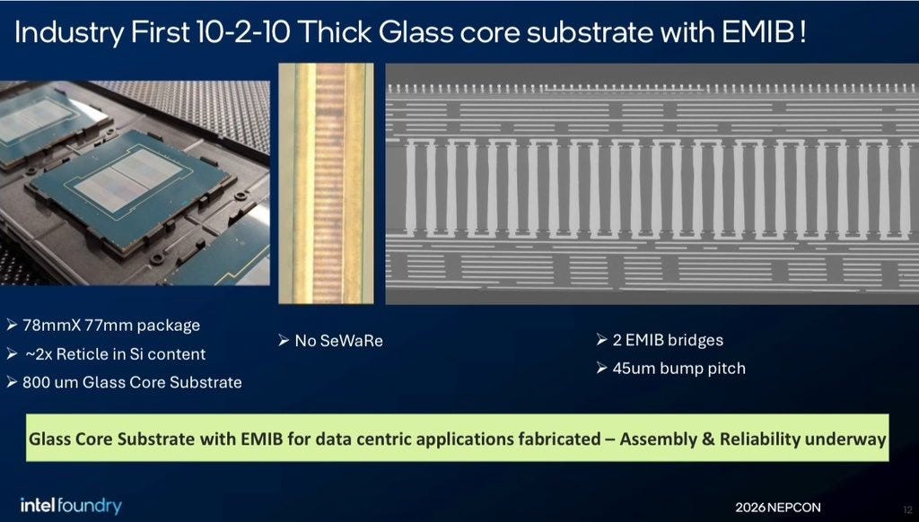
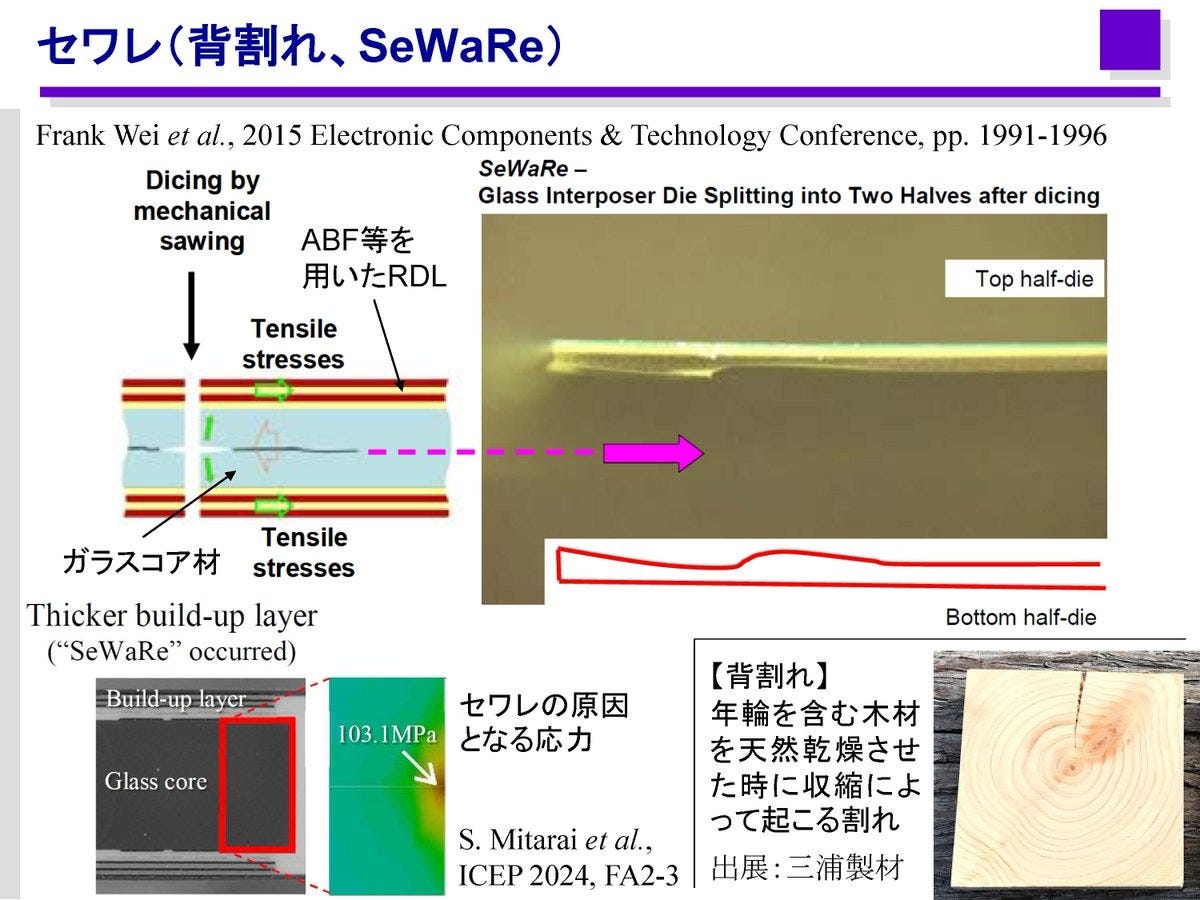
More importantly, Intel has solved the issue of “SeWaRe” - a Japanese term that refers to micro-cracking in glass substrates. It usually happens right through the lateral cross-section of glass -- kind of like when you pull apart the biscuit halves in an Oreo. Micro-cracking while drilling TGVs is an important problem that requires special techniques to deal with. One company holding a dominant position here is LPKF Laser and Electronics - a German company - whose Laser Induced Deep Etch (LIDE) process is capable of forming TGVs at scale. We’ll introduce another contender after the paywall.
The race to glass panels is just not an Intel vs TSMC race. Samsung and Rapidus are expecting to roll out glass interposer solutions as well.
For paid subscribers:
What this means to investors, and how the advanced packaging scene will play out
Two other supply chain names outside LPKF that are worth a look