
Why Faster PHY Design is the Low-Hanging Fruit in Custom HBM4 Base Die
A deep dive into HBM’s base die: covering DRAM structure, PHY functions, and how advanced interconnects like UCIe and next-gen PHYs from Marvell and Eliyan are defining the memory landscape.

Welcome to a 🔒 subscriber-only deep-dive edition 🔒 of my weekly newsletter. Each week, I help investors, professionals and students stay up-to-date on complex topics, and navigate the semiconductor industry.
If you’re new, start here. As a paid subscriber, you will get additional in-depth content. We also have student discounts and lower pricing for purchasing power parity (see discounts). See here for all the benefits of upgrading your subscription tier!
I’ve written a lot of articles on memory recently: why high bandwidth memory is so difficult to make, the case for high bandwidth flash, the packaging challenges involved, why memory is so important, and why there is an impending memory supercycle of which HBM is an integral part.
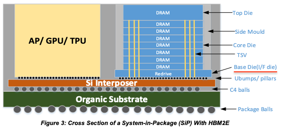
One important aspect that requires a detailed look is the base die that sits under the stack of DRAM die in HBM. This die is usually slightly larger than the DRAM chips stacked on top and ensures communication between the XPU and DRAM stack. From HBM4 onwards, the base die is going to get increasingly customized because its current implementation leaves a lot on the table in terms of performance, power and functionality.
In this post, we will look at why improved PHY design is the easiest upgrade possible using custom base dies designed for HBM4. In case you’re not familiar with the term, PHY is an abstraction in the Open Systems Interconnect (OSI) networking model for the physical layer where bits are transported from one point to another.
For free subscribers:
Basic Structure of DRAM Memory in HBM: How memory is addressed in HBM memory
Functions of HBM Base Die: The primary functions of HBM base die, and why PHY interconnect is a key element.
For paid subscribers:
Marvell and Eliyan: Benefits of using truly high-speed PHY built in advanced logic nodes, especially those designed at the 3nm node as demonstrated by Marvell and Eliyan.
UCIe: The option to use UCIe in HBM base die by licensing IP from Cadence/Synopsys.
Custom designs and key performance trends: Proprietary base die design from Nvidia/AMD, and latest trends in emerging die-to-die interconnect technology.
Read Time: 12 min
Basic Structure of DRAM Memory in HBM
First, let’s look at a basic example of how memory is accessed in HBM. The figure below shows HBM2e with 4- and 8-high stacks of DRAM.
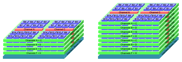
The 4-high DRAM is organized into eight channels A through H which can be operated completely independent of each other. Each channel is further divided into two pseudo-channels which are only partially independent of each other because they share the command clock and row/column address inputs. In HBM2e, each of these channels were read out on a 128 bit bus which resulted in a total number of 128 bits × 8 channels = 1,024 I/O pins. This is where the high bandwidth capability of this memory comes from. To get even more data capacity per channel, the 4-high stack is piled on top once more to make it 8-high.
In HBM4, the stack height is up to 16 and there are 32 independent channels (still two channels per DRAM die, and two psuedo-channels per channel) each of which is addressable by a 64-bit bus. This makes the total number of bits 64 bits × 32 channels = 2,048 bits over which data can be simultaneously accessed.
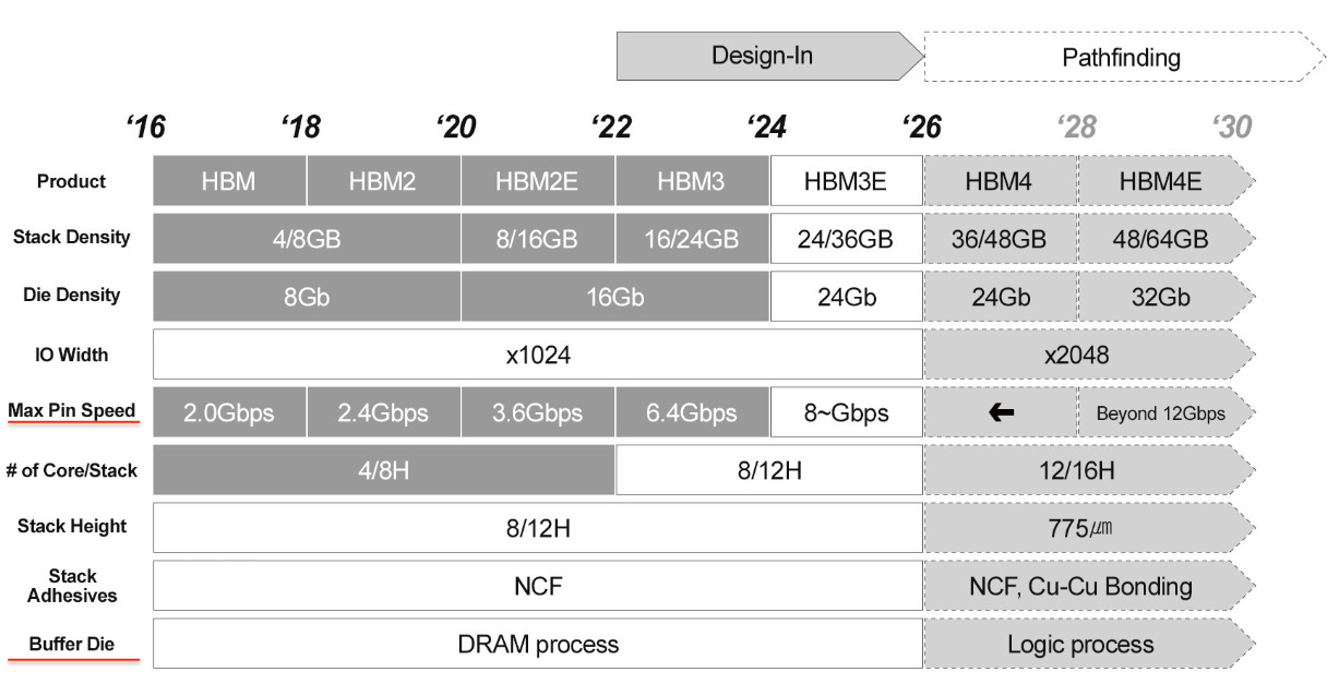
The table below shows the evolution of HBM architecture. Apart from the increasing number of I/O pins in every generation that is released every 18 months or so, two important metrics in this table are of note.
Speed per pin: It has steadily been increasing in every generation.
Buffer/base die: Up until now, DRAM process nodes have been used for the base die, but this is about to change in HBM4 and beyond.
Functions of a HBM Base Die
The main responsibility of the base die is to act as liaison between the XPU and the stacks of DRAM with addressable banks of memory organized into multiple channels. We can break down the base die into four different functionalities: Controller, Power Delivery Network, RAS, and PHY.
DRAM channel controller
The base die has logic that manages the read/write functionality to the various independent channels. It also manages DRAM refresh cycles and issues precharge and activate commands to prepare memory banks for read/write operations.
Power Delivery Network
The base die distributes power to the DRAM stack and as stack heights get taller, the IR-drop should be minimized by optimized layout of through-silicon-vias (TSVs) to efficiently deliver voltage to operate the memory banks. For example, SK Hynix put power TSVs all around the base die to reduce the overall voltage drop in HBM3e.
Repairability, Availability, Serviceability (RAS)
Due to the complexity of building HBM stacks, errors in DRAM cells or TSV failures need to be tested for, verified and repaired. The base die implements these functions through the Memory Built-In Self-Test (MBIST) block that identifies failed DRAM cells, verifies the fix using a soft-fix often by rerouting around them and then implements a hard-fix by blowing fuses around spare devices. Similarly, TSV failures need to be routed around as well using spares. The test and repair feature is essential to maintain higher yields in production and reliability in the field.
This block also monitors the health of the HBM system in real time, implements error-correcting-codes (ECC) to fix single-bit errors, manages refreshes to prevent rowhammer, and performs error logging for diagnostics.
PHY layer
The PHY layer is responsible for managing high speed signaling over the silicon interposer interconnect. It implements a high speed serializer-deserializer (SerDes), clock forwarding, forward error correction, clock and data recovery (CDR) and redriver functionality all in the hope of maintaining a wide open eye-diagram and low bit-error-rates in the interconnect performance. The data rate per-pin that is supported and the overall throughput of the HBM hinges on the high speed performance of this block. We will focus on this function in this article.
Due to the high I/O pin count (2,048 in HBM4), the PHY block must manage a large number of signal pins and usually occupies a significant area in the base die. There is a lot of value in optimizing the PHY design because reducing its size opens up more area along the XPU-HBM beachfront. Just shuffling bits in and out of memory is power intensive, and any optimizations for lowering power will add up in overall savings in system power because there are so many die-to-die PHY interfaces between XPU and multiple stacks of HBM.
Implementation of HBM3/e PHY
Even in the most recent generation, HBM3e, the base die is designed using a memory-centric process node. Memory-centric process nodes are named quite differently from standard logic transistors like 1a and 1b (or their greek equivalents), and not according to gate length like 5nm or 7nm. They consist of planar transistors because their primary function is to act as a switch to charge up or discharge the capacitor in a 1T1C cell (if you need background, read this) used in DRAM memory. These transistors are not built for speed and have physical gate lengths in the 10-15 nm range.
When a PHY is built on a base die that uses a memory-centric process node, the implementation is inherently inefficient: the physical area is larger, power consumption is higher than necessary, and speeds are restricted by transistor performance. However, memory makers like SK Hynix and Micron do not have internal access to a leading edge logic node to implement the PHY on a competent process node, and have to rely on external vendors such as TSMC. To own the entire HBM stack including base die, memory makers simply implemented high-speed digital functions on this ill-suited process node.
Samsung is a different story. Unlike their HBM competitors, they do have internal access to technologies that are true logic nodes. The likely reason they continued to use memory-centric nodes in the base die is because the performance was sufficient to meet JEDEC speed standards for HBM PHY. Going to a true logic node is expensive and is best avoided if unnecessary for performance.
With HBM4, the per-pin data rates are exceeding what memory-centric nodes can reasonably handle. The need for higher bandwidth is causing all major memory makers (maybe with the exception of Micron) to switch to a FinFET based technology with gate lengths in the range of 3-12nm for the base die.
After the paywall, we will dive deeper into the advantages of developing truly high-speed PHY on leading edge nodes, and what options exist to do so. Specifically:
Benefits from using Marvell and Eliyan IP for custom HBM
UCIe die-to-die IP from Cadence
Custom designs and key performance trends