
Grating Coupled COUPE for CPO, and Himax's Fragile FAU Moat
An engineering deep dive into TSMC's COUPE optical engine, explaining why the co-design position of Himax makes them critical near-term suppliers for NVIDIA’s CPO, but without a long-term moat.

Earlier this month, Citrini Research and Hunterbrook Media identified Himax $HIMX and FOCI (3363.TT) as potential key suppliers in NVIDIA’s co-packaged optics (CPO) supply chain - especially as related to TSMC’s COmpact Universal Photonic Engine (COUPE) that is the de-facto standard for the future of CPO in datacenters. Here, we will describe why Himax and FOCI have a near-term co-design position in COUPE but no long-term moat.
Citrini/Hunterbrook traced a trail through four patents (two Himax, one FOCI, one TSMC) and found that both Himax’s manufacturing patent and TSMC’s Fiber Array Unit (FAU) inspection patent describe a 22-channel configuration (standard fiber counts in optics are 12, 16, 24, and 32). The unusual but matching channel count across patents was considered the “smoking gun” that ties Himax and FOCI as a key TSMC supplier. PhotonCap has a patent-by-patent analysis that is worth reading for the full forensic detail. However, Irrational Analysis counters Citrini’s patent-centric approach stating:
There is zero discussion on coupling efficiency, polarization extinction ratio, or alignment tolerance.
The most dangerous analysis looks smart (check out these patents!) but actually delivers zero insight into the underlying viability of the tech.
These micro-lense assemblies are obviously for grating coupler attach. Grating couplers have high loss compared to edge couplers so the lenses better be damn good. Zero evidence this is the case.
In this article, we will look at the engineering details that are missing in the Himax/FOCI/TSMC conversation. We will cover:
Physics of edge vs grating couplers (free)
Implementation details of TSMC COUPE that makes it low-loss and well suited to CPO
Need for fiber array unit (FAU) co-design between TSMC and Himax/FOCI
Is Himax actually a good bet? How solid is their moat?
If you are not a paid subscriber, you can purchase just this article using the button below. You can find the whole catalog of articles for purchase at this link.
Physics of Edge vs Grating Couplers
Much of the discussion to follow requires an understanding of how light is coupled from a fiber into a chip, and how the entire flow of light works. We will cover this in some detail because it is necessary to understand what Himax+FOCI brings to the table, and how critical their technology is to the CPO supply chain.
There are two ways to get light on or off a photonic chip: edge and grating couplers.
Edge couplers
Edge coupling is the method of coupling light into the side of the chip. This is conceptually simple because the Photonic IC (PIC) has silicon nitride (SiN) waveguides into which light can be coupled from an optical fiber by narrowing the beam with a microlens, and using a waveguide taper where the fiber connects.
Since this only involves the light moving from one medium to another without really changing directions, most of the light energy couples to the PIC and loss is low. This is an oversimplification, but is sufficient here. Additionally, both wave-guiding media – optical fiber and waveguides on the PIC – support both transverse electric (TE) and transverse magnetic (TM) polarizations, which are wave oscillations of the electromagnetic field as light propagates.
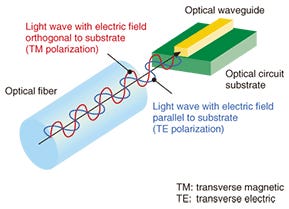
If the light transition from optical fiber to waveguide involves either TE or TM being attenuated, the coupler is said to have “polarization dependent loss, or PDL.” An edge coupler usually allows both TE and TM modes through, and has low coupling and PDL loss. But there are several downsides:
Limited beach-front density: Using only the edges of the PIC to couple light limits how many fibers can be placed around the periphery. This limits the number of ports in a CPO switch.
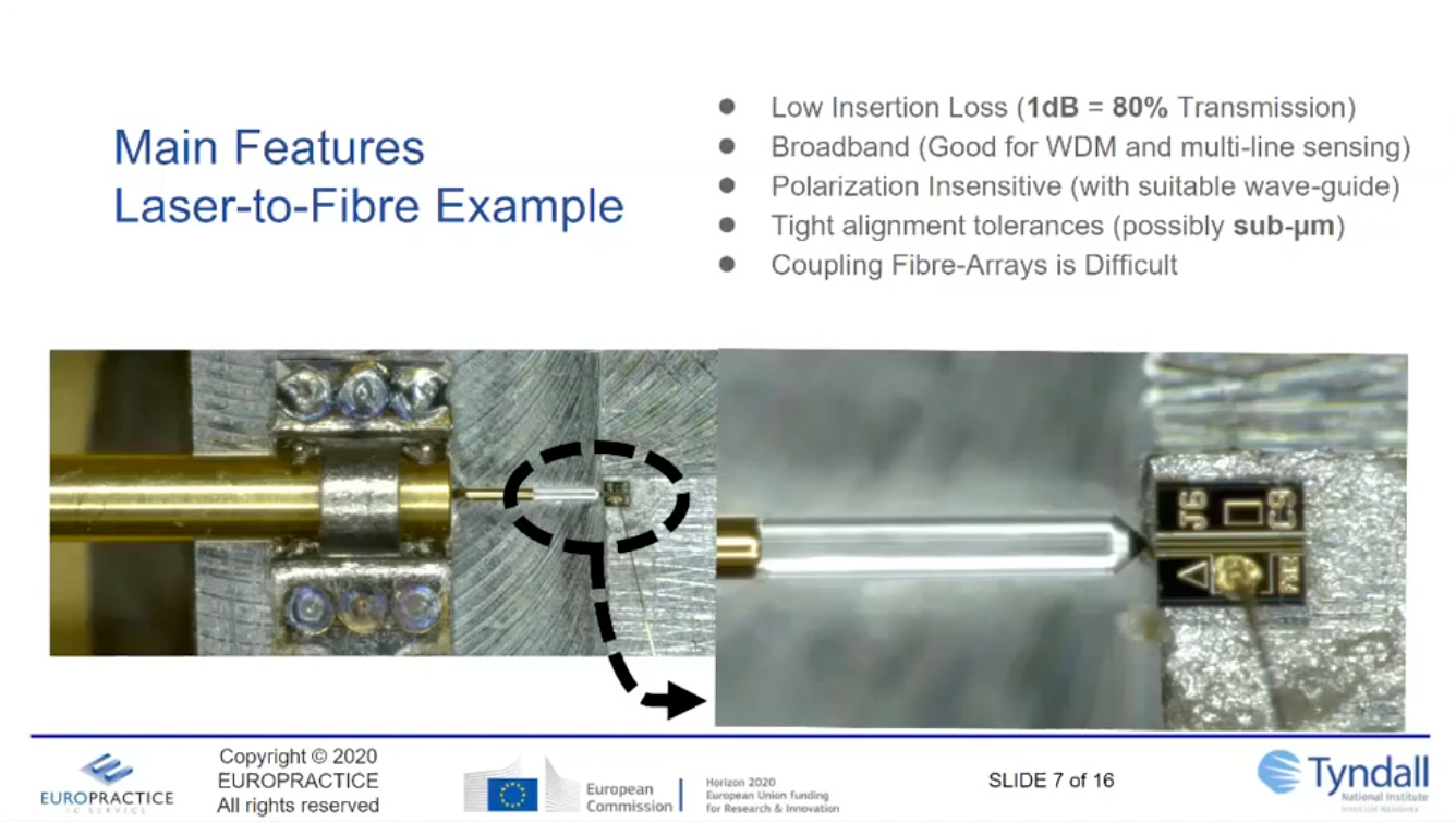
High alignment requirements: The optical fiber requires to be precisely aligned (<1 micron) to the waveguide taper so that all the low loss benefits are retained.
Singulation before testing: Each PIC must be diced from the wafer and tested by coupling from the edge. This makes testing low throughput and expensive.
Broadcom’s Tomahawk 4 (Humboldt) and 5 (Bailly) CPO switch chips are examples that use edge coupling to attach fiber to the chips. Below is a quick survey of recent edge couplers in C- and O-bands. The TE0 and TM0 modes both have very low loss, and the PDL is near zero which implies that both modes are coupled well.
Grating Couplers
A grating coupler allows light to enter or exit the PIC from the top surface rather than the edge. It is essentially a series of periodic etchings (grooves) on the surface of a waveguide. When light traveling through the waveguide hits these grooves, it scatters. By precisely spacing these grooves, the scattered light undergoes constructive interference at a specific angle, directed upward out of the chip. Conversely, light coming from a fiber at that same angle will interfere constructively to “drop” into the waveguide.
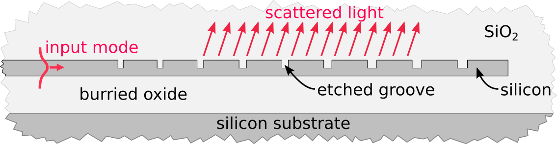
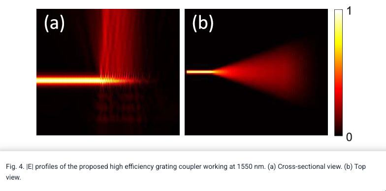
Here is a simulated side and top view of the field that transitions from a waveguide to scatter vertically. It is important to note that scattering happens in both directions. Even though one direction is predominant, the loss of light on the other side contributes to loss. We will revisit this point later in TSMC COUPE.
There are some immediate advantages that become apparent in grating couplers:
Beach-front area: The entire 2D surface of the chip is available to connect fibers, which greatly increases the density of fiber that can be connected to a chip compared to using the edge alone.
Lower alignment requirements: Grating couplers provide significantly relaxed fiber alignment tolerances compared to edge couplers, typically featuring tolerances of 2-4 microns either way from the center.
Wafer level testing: Since light comes out of the top of the chip, PICs can be tested before dicing, greatly simplifying the process and increasing throughput.
In spite of these advantages, there are some downsides.
Higher loss: Grating couplers are inherently higher losses due to the scattering effects that occur in the grating structure. Lots of research has been done to minimize this.
High PDL: Grating structures only work for one of the polarizations, while the other undergoes high loss.
The impact of high loss in gratings implies that link budgets are smaller when going to faster data rates, and everything that follows – the microlenses, prisms, and FAUs – must all be optimized for the lowest loss possible. High PDL implies that data rate cannot be doubled easily by putting information on each polarization (polarization multiplexing), which becomes a limiting factor as we look to scale data rates higher. Here is a recent survey of grating couplers if you’re interested.
After the paywall, we discuss:
The engineering behind TSMC COUPE, including the implementation details that makes it low-loss and well suited to CPO.
Why the fiber array unit (FAU) needs to be a co-design between TSMC and Himax/FOCI
Discussion on whether Himax is actually a good bet, and how solid their moat is.