
IMS 2025: AI for RF, Heterogenous Integration, 100 GHz+ Systems, RF GaN
Conference highlights and key takeaways from the 2025 International Microwave Symposium held in San Francisco - the world's premier conference for RF/microwave engineering.

Welcome to a 🔒 paid-subscriber technical conference update 🔒. The expenses for attending this conference were covered thanks to the support of my paid subscribers. I truly appreciate it.
If you’re a free subscriber, I have a value proposition for you.
Even though I encourage you to attend conferences whenever you can, there are times when travel just isn’t possible for all sorts of reasons. Sometimes it’s simply too much extra work — visas, flights, hotels, registrations, jet lag.
Here’s the thing: I do all of that for you and you get all the insights through the lens of someone who has worked in the industry for 15 years.
By upgrading to a paid tier, you’ll get access to all the insights from IMS 2025 and other conferences I attend — ISSCC 2025, IEDM 2025, and possibly more — all from the comfort of your chair, for a fee you can probably expense to your employer (paid subscription dollars are far less than conference travel costs). You’ll also get full access to the deep-dives in the archives, plus everything I publish in the future.
Send this email to your manager and get them to expense an annual subscription, or get group discounts for your org. Both your employer and you stand to benefit.
If you’re new here, check out the start page to get oriented. We also have student discounts and lower pricing for purchasing power parity (see discounts).
The 2025 International Microwave Symposium (IMS) wrapped up last week at the Moscone Center in San Francisco. As the flagship conference for RF and microwave engineering, IMS draws top research groups, major industry players, and a sprawling exhibition floor with over 500 booths. If you work in RF, this is the one conference you should try to attend.
I hadn’t been back since presenting my PhD work in 2011. Fourteen years later, it was good to return — catching up with old colleagues, reconnecting with industry friends, and meeting several readers of this newsletter in person. A highlight: my PhD advisor, Prof. Kamran Entesari, was elevated to IEEE Fellow this year. Well deserved, and I’m glad I was there to witness it.
In this post, I’ll walk through the major themes I saw at the conference, highlight a few notable papers, and share the key takeaways you might want to keep in mind from this event.
Quick note: There were far too many interesting papers to cover them all. This post is simply a collection of what I was able to attend and what I think represents a developing area — a personal choice. It does not reflect in any way on the quality of research in the papers I have left out.
For free subscribers:
AI-Enabled RFIC Design: How optimization and generative AI methods are being applied to design passive devices that defy traditional intuition, often delivering better performance than conventional approaches, and reshaping how we might think about circuits in the future. I’ll go over some of the papers, workshops, and start-ups pushing the boundaries in this new and promising field.
For paid subscribers:
Heterogeneous Integration: Choosing the right technology for the right function will be essential for achieving cutting-edge circuit performance in the future. There are several papers that show this approach working well in practice.
MIT: GaN + CMOS for power amplifiers
ST Microelectronics: SiGe + LDMOS SOI for sub-6 GHz power amplifiers
PseudoLithIC: InP + CMOS for 70-80 GHz amplifiers
100 GHz+ Systems: From D-band (150 GHz) to J-band (250 GHz): Exploring circuits and systems above 100 GHz offers clear advantages. The spectrum is relatively open, and wide channel bandwidths enable wireless speeds beyond 100 Gbps. There are tough challenges though, and overcoming them usually demands extreme engineering.
Nokia-Bell Labs: D-band Radio-on-Glass for multi-km wireless backhaul
NTT: J-band amplifier with 70 GHz bandwidth, 30 dB gain, 280 Gbps data rate.
Phased-Arrays and Beamforming: There is increased interest in this area for SATCOM applications and sensing.
IBM Research: Fast Steering of Arbitrary Beams with Phased Arrays
GaN for RF Applications: There was a lot of buzz around GaN and its future in RF systems, both in the exhibition and at technical talks/workshops.
Fraunhofer IAF: D-band MMIC T/R module using 70um GaN HEMT
Panel Sessions, Exhibition and Conclusion
Read time: ~20 minutes


AI-Enabled RFIC Design
The most exciting theme of the conference, by far, was the use of AI in RF design. The planning committee saved it for last technical session before the closing keynote and drew the largest audience of any talk I attended. The speaker lineup reflected the significance of the topic, with presentations from top research groups at Princeton (Prof. Kaushik Sengupta), UT Austin (Prof. David Pan), USC (Prof. Hossein Hashemi), ETH Zurich (Prof. Hua Wang), and Caltech (Prof. Ali Hajimiri).
The session focused on designing matching networks, filters, and other passive components that aren’t easily described by traditional templates like spirals or stubs. Machine learning methods were used to explore arbitrary metal shapes that produce the target electrical response. And for the first time at a conference like this, no one asked how it worked — just that it did, and in fascinating ways.
Pixelated Matching Networks
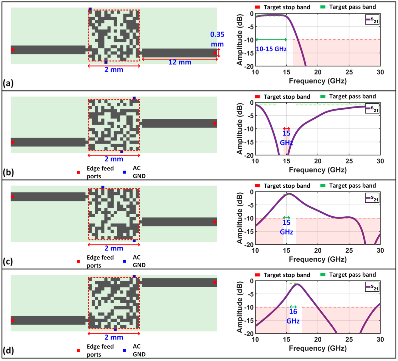
A paper titled “Algorithmic Design of Nonintuitive On-Chip Multilayered Passive Networks” from the University of Southern California won 1st place in the RFIC student paper competition. Similar to the earlier work from Prof. Sengupta’s group where power amplifier matching networks could be implemented with a QR-code like passive structure, this work extended the idea to implement them on three metal layers, where the sheer number of design possibilities explodes.
The paper used an explore-and-exploit approach using direct binary search (DBS) and binary particle swarm optimization (BPSO) methods; these are traditional optimization methods rather than machine learning algorithms. BPSO broadly covers the solution space in a coarse manner, and DBS uses an exploitative approach to quickly hone in on the optimal design. In the circuit example shown below, the bandpass filter could be made approximately 60% smaller by simply reducing the pixel sizes, all without sacrificing electrical performance.

Another important advantage is the ability to achieve identical circuit functionality with various pixel arrangements. This feature inherently makes the design difficult to reverse engineer, providing a natural layer of intellectual property protection. Additionally, each design can employ unique pixel patterns. If unauthorized copies appear elsewhere, tracing the distinct patterns back to the original source becomes straightforward, effectively creating a built-in mechanism to track IP leaks.
DALL-EM: Diffusion-based generation of passive circuits
This was another intriguing study from Professor Kaushik Sengupta's group at Princeton University titled "Dall-EM: Generative AI with Diffusion Models for New Design Space Discovery and Target-to-Electromagnetic Structure Synthesis," which blew up on X when I posted the chart below. They used generative AI to generate passive circuits with diffusion models, similar to how OpenAI's DALL-E and MidJourney make images.
It works by giving a generative AI the intended passband and stopband requirements, and the AI will create a passive network that meets those parameters. Because of the random nature of generative approaches, several layouts may have identical electrical performance. This also enables the design obfuscation strategy, which we described before, allowing design teams to safeguard their IP.
The image above illustrates various passive circuit types (low-pass, band-pass, and band-stop) generated using diffusion models. At first glance, the metallic layouts don’t intuitively reveal how they achieve their electrical characteristics — their behavior is entirely non-obvious.
One intriguing feature of this research is the inclusion of a controllable “design knob,” which adjusts spatial entropy, effectively setting the complexity of the generated structures. Low-entropy settings produce classical designs, characterized by smooth and continuous metallic features reminiscent of traditional transmission lines or stubs. In contrast, high-entropy settings lead to more intricate, pixelated patterns resembling QR codes. The style of design chosen could depend on manufacturing constraints, yield considerations, or repeatability requirements. Thanks to Prof. Sengupta for sharing this image on LinkedIn and explaining how this process works!

Notably, this work received second place in the IMS student paper competition.
Workshops
The Sunday workshop on AI-enabled design methods for RF had one talk that stood out in particular — Prof. Fabio Passos’ “WSC3: AI/ML Techniques Supporting the Design Automation of RF/mm-Wave Circuits.” Unlike the more radical end-to-end approaches showcased in the main technical sessions, Prof. Passos’ work focuses on integrating machine learning into conventional design flows. This makes it practical for real-world, industry-grade designs, where trusted design flows have existed for decades.
His method follows a three-part strategy. First, use ML-based surrogate models to accelerate electromagnetic simulations. One example is PACOSYT, a passive synthesis tool built around machine learning. Second, apply optimization techniques to explore large design spaces efficiently. And third, incorporate parasitic and yield-aware layout co-design early in the process to reduce the number of design iterations.

A lot of AI-driven RF design research leans toward building entire circuits end-to-end using neural nets or generative models. But that doesn’t always scale, especially when designing complex systems like a full transceiver. In practice, design is always broken down hierarchically, block by block, and then stitched together. Prof. Passos argues that ML-based flows should follow the same structure, which is a more tractable way to approach large designs.
AI-RFIC Startups
Two startups at the exhibition stood out for their use of AI in MMIC circuit design: RapidRF and ZapRF. Both offered platforms that promised to speed up the traditionally long and iterative process of analog design.
At RapidRF’s booth, I tried out their design tool firsthand. Their interface was a simple web form. You enter your amplifier specs — gain, noise figure, linearity, and frequency range — and submit the request. For this trial run, I tried specifying a GaAs low-noise amplifier operating at 14 GHz; details shown below including the performance that was achieved in about 3 hours of design time.
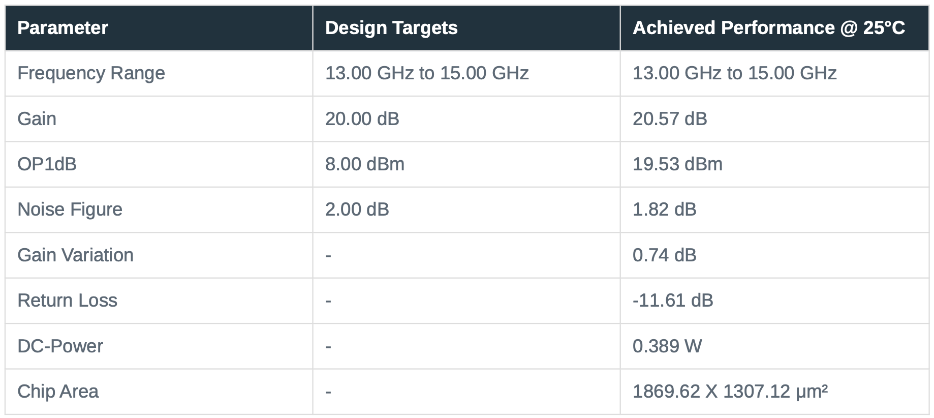
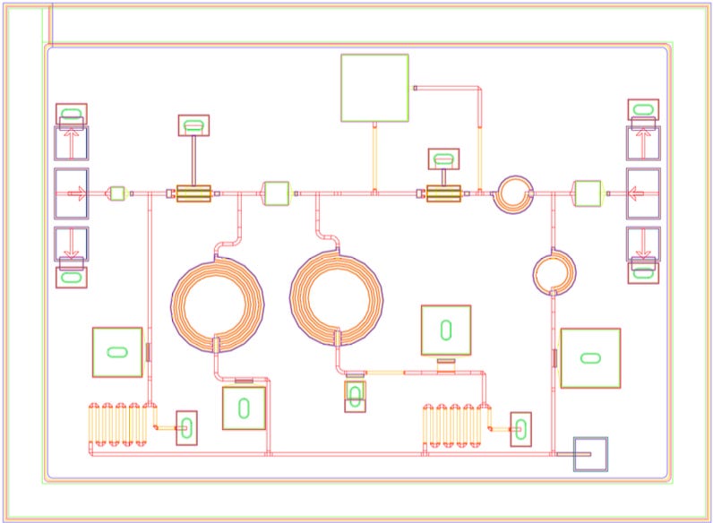
The design run also provides a GDS-ready layout as shown below, along with some plots of the amplifier performance. If I understood correctly, the simulated performance includes the EM simulation of the passives co-simulated with transistor compact models.

At the outset this seems quite impressive. However, the design needs of the industry are often much more sophisticated than a simple spec sheet, but I imagine this design flow will evolve with time. Specifying chip size limitations, setting up custom simulation setups and measurements, and injecting company specific IP are all required for the complete usefulness of this tool.
Established vendors like Keysight also showcased AI-assisted design flows, signaling that this approach is gaining broader traction. I’ll continue tracking these developments and share what I learn on this newsletter.
