Noise in Cascaded RF Systems
How total noise is calculated in an RF system that has a cascade of components, each with its own gain and noise.
Hey, I’m Vikram 👋! Last week, we had some discussions in the Substack chat about how to create an online community for RF. We could do something asynchronous like a forum, or synchronous like discord or slack. Live sessions on LinkedIn or other platforms is possible too. Let me know if you’re interested in something like this via Substack chat or email.
Due to LaTeX equations, this article is best viewed in a browser.
If you are enjoying this newsletter, please leave me a testimonial here. It takes less than 1 min.
Click ❤️ on Substack if you enjoyed it, leave me a comment or share this article. Making noise helps grow this newsletter! 🙏
Over the last few months, we have been collecting bits and pieces of concepts related to RF systems. Here, we will put a few of those learnings together.
We discussed at length about the different kinds of gain in an RF amplifier, the sources of noise in MOS devices, and developing an intuitive feel for nonlinearity of a system. We also looked at the history and architecture of the RF superheterodyne system, and how to choose the right frequencies to prevent images.
In this article, we will learn about gain, noise, and their interaction when RF components are cascaded to build a system.
Read time: 9 minutes
Cascaded Gain
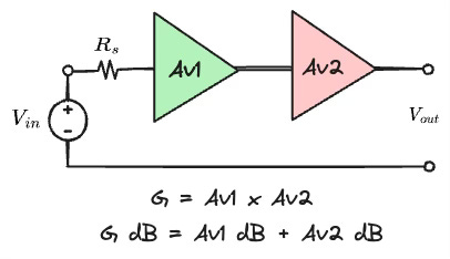
We spoke about gain extensively in a previous article, so we won't go too deep here. We will limit ourselves to understanding what happens when two RF components having gain are cascaded as shown in the figure.
The voltage or power gain at the output is simply a multiplication of the gains of each individual block. In decibels, cascaded gain is the addition of the gain of each block. If one or more of the blocks shows attenuation or insertion loss, the "gain" of the block expressed in decibels is negative.
This makes it quite simple to add and subtract the gain of each block in a cascaded system to calculate overall gain.
Input-Referred Noise
In a previous article, we looked at sources of electronic noise. We use a different perspective from a system point of view. We are not concerned with the actual source of noise, but only metrics that define how noisy a circuit is.
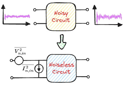
To do this, we use the concept of input-referred noise. It is represented by a series voltage source and a shunt current source connected at the input of a noiseless circuit. The composite noise from each of these sources, in presence of the noiseless circuit, is equal to the noise from the original circuit. The voltage and current noise sources are often correlated too.
Why input-referred? Depending on the gain of the circuit, the noise at the output is also amplified. This makes it difficult to compare noise performance of circuits with different gain. The simpler way is to define noise at the input of the circuit.
How do we find the values of the voltage and current noise sources?
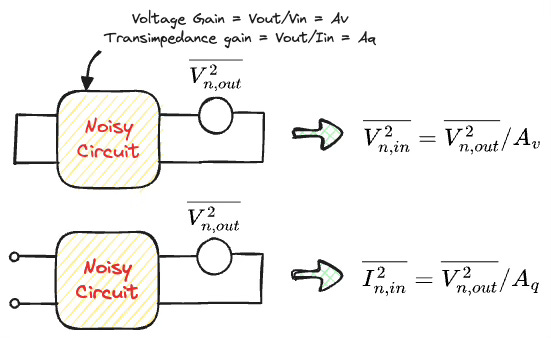
Voltage noise: Short the input terminal to eliminate current noise. Measure the output noise, and divide it by the voltage gain (Vout/Vin) to obtain input-referred voltage noise.
Current noise: Open the input terminal to eliminate voltage noise. Measure the output noise, and divide it by the transimpedance gain (Vout/Iin) to get input-referred current noise.
Noise Figure
For simple circuits, the concept of input-referred noise works nicely. For complex RF blocks, finding voltage and transimpedance gain is not trivial. Instead, we can define another metric in terms of signal to ratio (SNR).
If an amplifying RF block has a signal at its input terminal, the amplification increases both the signal and noise by the same level at the output. In terms of SNR, nothing has changed from input to the output: SNRin = SNRout. This is only assuming that the amplifier itself did not contribute any noise.
In reality, in addition to the amplification of input noise, there is noise generated by the RF block. As a result, the SNRout is lower than SNRin, which leads itself to a simple definition of noise in terms of Noise Figure (NF) which is given by
Noise figure is most often expressed in terms of decibels by taking 10*log(NF). A noiseless circuit has a NF=1 or 0dB. We will derive this value in the next section.
Importance of Source Impedance for Noise Figure
Signal-to-noise ratio is not always convenient to calculate and we can look at noise figure in a more intuitive way if we were to express it only in terms of noise voltages. At least for single RF blocks, we know that the relationship between the input and output signal is its voltage gain. NF is a metric that defines how much excess noise has been added by the circuit block in addition to the noise increase due to voltage amplification.
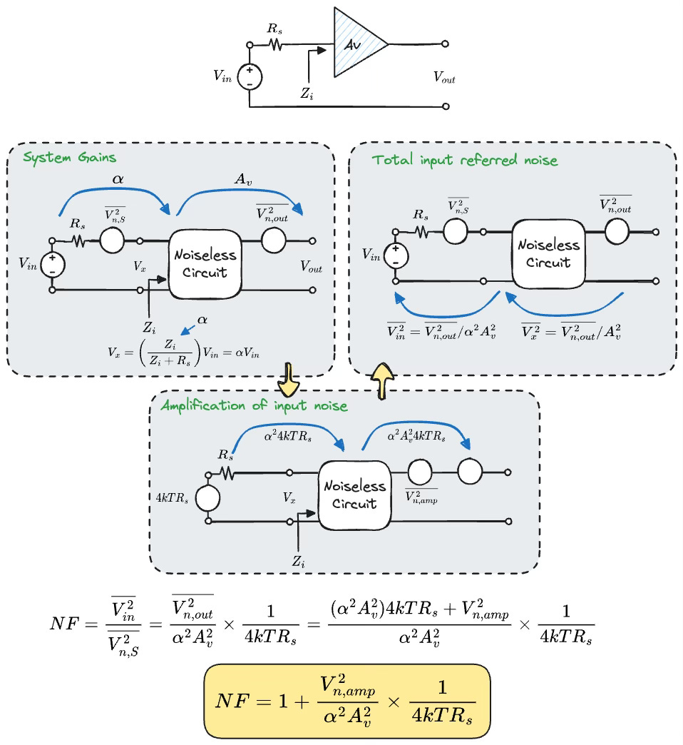
Let us dive in a bit deeper with a simple example. Take the case of an amplifier with gain Av and input impedance Zi. This amplifier is noisy and produces an equivalent output noise voltage Vn,out. The amplifier is fed with a supply whose input resistance is Rs, generating a thermal noise 4kTRs. This scenario is shown in the figure below.
System Gains: Due to the differing impedances Zi and Rs, there is voltage division at node X whose ratio is expressed as ɑ. So any voltage Vin at the input, is reduced by this factor and appears at the input terminal of the amplifier with a voltage ɑVin. This input voltage is further amplified by the amplifier by Av so that the output signal is ɑAv times Vin.
Amplification of input noise: The thermal noise power of the source resistance is 4kTRs. Due to the mismatched impedance at the input, the noise power appearing at the terminals of the amplifier is ɑ-squared times 4kTRs, which is further amplified by Av-squared due to the gain of the amplifier. This is the noise at the output due to input thermal noise alone. In addition, the amplifier adds voltage noise due to its own noisy internals, which adds to the thermal noise at the output.
Total input-referred noise: The total noise at the output can be input-referred all the way back to Vin. First, the total output noise is divided by Av-squared, and then again by ɑ-squared. A useful observation is that the input-referred noise is low if:
The gain Av of the amplifier is high, or
ɑ is high, which happens if the input impedance of the amplifier is much greater than Rs. If Zi is high enough, ɑ approaches 1.
We can then calculate NF as the ratio of the total input-referred noise to the noise due to the source resistance at the input. It is clear from the equation that the lowest NF can go is unity.
It is important to recognize that the NF depends on the relative mismatch of the input of the amplifier to the source resistance Rs, as represented by ɑ. When we visit amplifier design in a future article, it is important to remember this: the noise performance of the amplifier depends on the choice of the source matching network.
Noise Figure in a Cascaded RF System
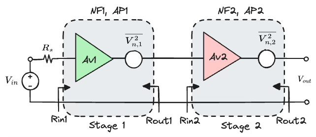
Now let us add another stage of amplification to the system as shown in the figure.
The gain of each stage is Av1 and Av2, respectively. Each amplifier has an input resistance Rin1 and Rin2, and output resistance Rout1 and Rout2. For simplicity, let us assume that the amplifier impedances are purely real. In reality, they are not, but the imaginary parts can be tuned out with passive matching components.
By using the same principles in the preceding section to calculate NF, the composite NF of the system can be shown to be
Here, NF1 and NF2 are the noise figures of the first and second stage, respectively. AP1 is the "available gain" which we defined in an earlier article as
Available Gain: The maximum output power you can get from the device, when you provide all the power from the source to it.
The maximum output power is only possible when the specific amplification stage is presented with a matched load at its output. Similarly, all the source power can only be obtained if the input of the amplification stage is matched to the source. Basically, available power is about as much power as you can get from the amplifier in matched conditions.
If you are up to a challenge, you can use the principles of NF in this article along with the right definition of available power to derive the above equation yourself (or just look at chapter 2.3.5 in RF Microelectronics by Behzad Razavi.)
We drew symbols for an amplifier just to explain the idea, but in reality, the cascaded blocks can really be anything - amplifier, mixer, etc., or even passive devices like attenuators and filters. This equation applies to all such cases.
Friis Equation
But without attempting too much math, we will extend this to 'n' RF cascaded blocks and write down what is known as the Friis equation for a general case of cascaded RF components each with its own NF and available gain.
The implications of this equation are quite significant for RF system design:
NF of 1st block is important: Most of the total NF comes from the NF of the first component in the signal chain. This is why low-noise amplifiers (LNAs) are placed as close as possible to the antenna. Any losses in filters and switches before the LNA have massive impact on the noise of the overall system. Such RF front end components that come before the LNA are designed to have extremely low loss.
Gain of the 1st block should be high: As long as gain of the first block AP1 is high enough, the NF of the second block in the chain matters significantly less. Each subsequent block in the chain is decreasingly significant to the overall NF.
Noise amplifies due to loss: If the available gain is less than unity, then the noise of the following stage is amplified when referred back to the input of that lossy stage.
For a passive component with insertion loss, the noise figure of the component is equal to the insertion loss. For example, if there is a filter with 1 dB insertion loss followed by an LNA with 2 dB NF, Friis' equation says that the total NF is 3 dB.
The Friis equation is useful for a qualitative understanding of how cascading affects total NF. It is practical when building discrete systems where the manufacturer provides the specifications of each block in a data sheet. But sometimes, the available gain and noise figure of each stage may not be known, especially for integrated circuits where the interface between the stages is not matched. In such cases, it is hard to use this equation directly and you're better off using EDA tools to evaluate total NF.
📚 References
B. Razavi, RF Microelectronics 2nd ed., Chapter 2.3.5.
The views, thoughts, and opinions expressed in this newsletter are solely mine; they do not reflect the views or positions of my employer or any entities I am affiliated with. The content provided is for informational purposes only and does not constitute professional or investment advice.

Thanks Vikram, nice article. When calculating the input current and voltage noise, shouldn't we divide by the squared gains?