
Plastic Cables for AI Clusters: Can Point2’s E-Tube Disrupt Copper and Optics?
A deep dive into dielectric waveguides, the company behind them, performance compared to copper and optics, and whether hyperscalers will actually adopt this “third path.”

Welcome to a 🔒 subscriber-only deep-dive edition 🔒 of my weekly newsletter. Each week, I help investors, professionals and students stay up-to-date on complex topics, and navigate the semiconductor industry.
If you’re new, start here. As a paid subscriber, you will get additional in-depth content. We also have student discounts and lower pricing for purchasing power parity (see discounts). See here for all the benefits of upgrading your subscription tier!
There is a grey area in AI datacenter interconnects where copper is not good enough but optics is overkill. To address “mid-reach” applications in modern datacenters, a new innovative solution exists in this space that is not nearly talked about enough: plastic dielectric waveguides, and Point2 Technologies is a startup that has an interesting solution in this space.
In this post, we will look at e-Tube interconnect technology in detail, and discuss how it measures up against copper and optical interconnects. We will discuss:
Copper’s reach problem: Where copper falls short as an interconnect for datacenter scale-up.
Optics’ power problem: Why everyone is avoiding optics because it is overkill for scale-up.
Introducing Point2 Technologies: A brief introduction to the the company, its leadership, and investors.
Understanding e-Tube: Detailed explanation on how the interconnect works, and the components are constitute it.
For paid subscribers:
Microstrip to Waveguide Bottleneck: An in-depth look into the electromagnetics of the transition, and why it limits the performance of the interconnect.
Where CPO fits in: Why and how co-packaged optics is a competing technology to e-Tube.
e-Tube vs. AEC vs. CPO: A detailed comparison based on power, speed, latency and reach, and where each technology shines.
Closing Thoughts: A few odds and ends on what it would take for this technology to take center stage.
Read time: 13-15 mins
Copper’s Reach Problem
Passive copper cables are great because they consume almost no power, have near-zero latency, and work great at distances of up to 3-5 meters at 50G PAM4 (4-level pulse amplitude modulation) signaling rates. As interconnect speeds have reached 200G PAM4, passive copper reach drops to under 1 meter. Reach can be extended by using thicker copper cables (lower AWG gauge) but this quickly add weight and causes problems in routing a large number of cables (a single AI rack has 2 miles of copper cables.)
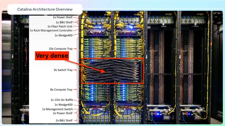
Take a look at Meta’s Catalina pod below. The thick copper cables running between switch trays in adjacent racks is very dense. This makes cooling difficult, and cable replacements cumbersome.
Scale-up interconnects are also becoming issue within an AI rack. A rack is typically 2 meters tall and the interconnect technology should ideally be able to connect GPUs and networking gear together at this distance with extra margin for handling.
The solution to extend reach is to use active copper cables (ACC) which use a redriver and equalizer to overcome the loss of the copper cable. The extra electronics adds a little bit to the power consumption (1-2W at each end), but is still very low latency (~1-2 ns). This solution extends copper reach to about 3 meters at 100G PAM4 rates, but reach again becomes a problem at higher speeds and/or longer distances.
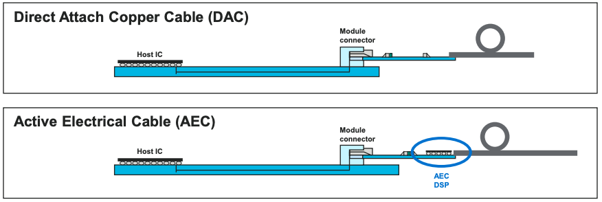
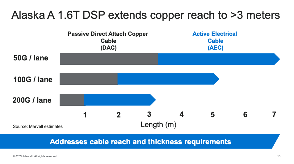
A more advanced method is to use active electrical cables (AEC) which implements DSP-based retiming, forward-error-correction (FEC), and full clock data recovery (CDR). This method gives the best performance possible out of a copper cable which comes at the cost of power consumption (~10W at each end) and added latency (20-100 ns). As speeds reach 200G per lane, the reach is still about 3 meters as shown in Marvell’s marketing slide showing the capabilities of their Alaska A retimer for AEC. This retimer chip is built on a 5nm process node and can deliver 1.6 Tb/s with 8 parallel lanes up to 3m. Alphawave (to be acquired by Qualcomm) also has a similar solution. The AEC solution roughly translates to ~6 pJ/bit energy consumption at these data rates.
When we transition to 400G PAM4 per lane sometime before 2030, it is likely that copper is not an option any more; it is getting hard even with retiming circuits. The obvious solution would be to transition to optical fiber for scale-up in a rack.
Optics’ Power Problem
Optical cables have enormous reach because it relies on the propagation of light through glass fibers instead of resistive copper wires. This is why they are used for subsea transcontinental connections. But AI datacenters have been avoiding it for scale-up applications within a rack primarily because of the power requirements of optical systems. At 2024 Nvidia GTC, Jensen Huang said:
If we had to use optics, we would have had to use transceivers and retimers. And those transceivers and retimers alone would have cost 20,000 watts, 20 kilowatts of just transceivers alone, just to drive the NVLink spine.
To understand where the power usage comes from, look at the picture below that shows the optical transceiver embedded in an Octal Small Form-factor Pluggable (OSFP) connector.
The laser source is commonly an externally modulated laser (EML) that consumes ~10W all on its own. The DSP converts parallel-to-serial data conversion (SerDes) and converts the digital signal to an analog one, which is then amplified by a driver in the transmit side and transimpedance amplifier on the receive side. For example, Broadcom’s latest Siam3 200G/lane optical DSP, built on a 3nm process node, consumes ~23W of power. Thus, the whole circuit can consume 30W per connector, which is easily three times what AEC consumes. In addition, the use of a DSP still adds latency. For a 1.6Tb/s, optical DSP solutions typically have energy usage in the range of ~20 pJ/bit.
The long reach of optics is overkill for hooking up GPUs in a single rack. In an era where AI datacenters are constrained by power more than anything else, the high power usage of optics is unacceptable. Still, co-packaged optics (CPO) holds promise. We will revisit this beyond the paywall.
Introducing Point2
Point2 Technologies is a Bay Area startup that proposes a unique solution: convert digital data into RF signals, couple it into a dielectric waveguide made of plastic, transmit it across the plastic tube and decode it with a receiver on the other end. They call this e-Tube technology and we’ll look at the exact details of how this works in the next section. For now, we’ll briefly introduce Point2 as a company.

Point2’s main goal is to extend the reach of interconnects using mixed-signal SoC solutions. Since 2016, Point2 has been developing both e-Tube technology and retimers for high speed AEC interconnects. Their CEO, Sean Park, was previously a Director at Marvell where he led RFIC design. His next stint was at TeraSquare as CEO, which was eventually acquired by Gigpeak in 2015.
Point2’s notable investors include Molex Ventures and Bosch Ventures, who recently funded their Series B round of totaling $22.6 million in 2024. Their interest primarily stems from the fact that Molex is a big supplier of connectors into the AI datacenter market and Bosch is heavily involved in the automotive market. Most recently, Foxconn Interconnect Technology (FIT) subsidiary has partnered with Point2 to further develop their e-Tube technology for 1.6 Tb/s and 3.2 Tb/s AI cluster interconnects.
Inside E-Tube: How Plastic Dielectric Waveguides Work
In 2020, KAIST and Point2 published a paper in Nature (open access) describing e-Tube for interconnects. Below is a condensed version of how the technology works.
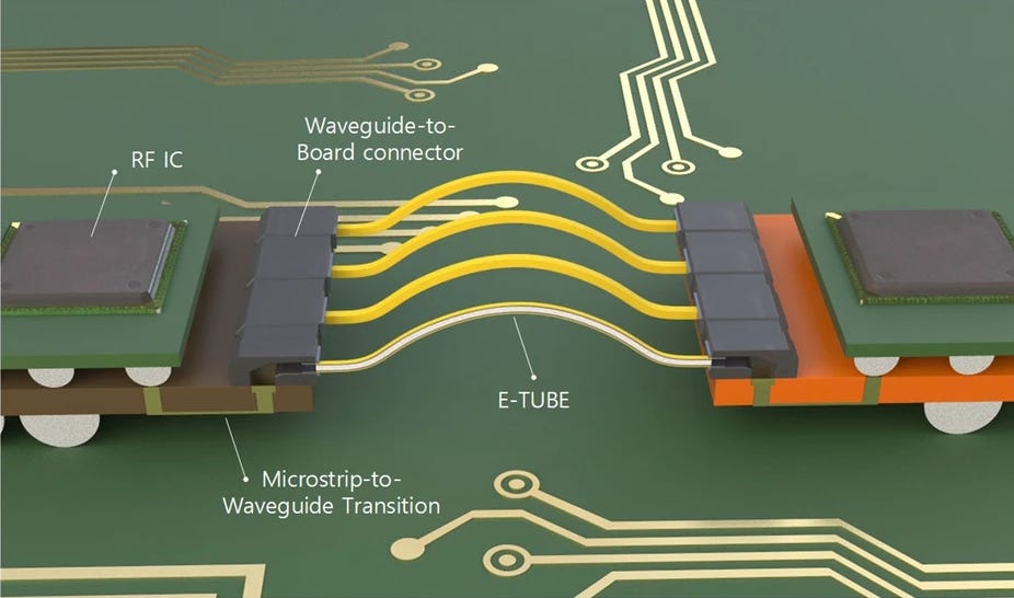
A diagram of the point to point interconnect is shown below. It consists of digital data being input to a mmWave RF transmitter which modulates the information and upconverts it to mmWave frequencies in the V-band range (~70 GHz). Once the RF signal exits the RFIC through the solderball, there is a microstrip-to-waveguide transition that couples the RF energy into an e-Tube. At the other end, another transition converts the received signal into a microstrip signal that feeds a mmWave receiver which converts RF signals into digital signals. We’ll look at each component in greater depth next and dive deep into where the benefits and shortcomings lie.
RFIC System on Chip (SoC)
As difficult as mmWave sounds, making the RF SoC transceiver (Point2’s brand is called UltraWave) is actually the easier part of this problem. Other than the detailed RF engineering needed, which is quite run of the mill for an experienced RFIC design team, the design process is actually straightforward. The published paper uses a 28nm RF CMOS process, but a more modern implementation can even go to 22nm or lower. Silicon-Germanium (SiGe) processes are also commonly used for mmWave applications. All these process nodes are lower cost compared to leading edge nodes used in optical DSP chips. They are also well established, produce high yield, and can be manufactured on 200/300mm wafers without any special processing.
In terms of power budget, the lack of advanced DSP will make it more energy efficient. Low-power RF design is also well understood especially in the context of circuits for mobile handsets. For good pJ/bit performance, it is critical that the waveguide transitions have lower loss by better mode matching. We will look at this in detail in the next section. Since conversion and transmission of data is entirely analog, the additional latency introduced will also be much lower than DSP-based methods.
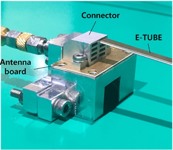
When the active circuits are combined with e-Tube interconnect, it can all be included in OSFP plugs as shown in the picture below to be compatible with industry standard pluggables. This is called Active RF Cable (ARC) technology.

e-Tube Plastic Waveguide
The original 2015 implementation of the e-Tube waveguide was essentially a (filled) plastic straw through which RF signals are transmitted. However, instead of using a pure dielectric which is prone to leaking energy, the plastic straw is wrapped with metal to confine it. However, using a circular cross section waveguide makes the interconnect inherently band limited due to propagation of TE11 as dominant mode (more on this coming up.)
But the modern implementation in 2020 shows that the e-Tube is more of a parallel-plate waveguide with rectangular cross-section: two metal plates sandwich a low-loss dielectric such as polytetrafluoroethylene (PTFE) as shown below. The cable is about 3.5mm wide and 0.6mm thick, which makes it low profile. Remember that width number; it will tell us a lot.
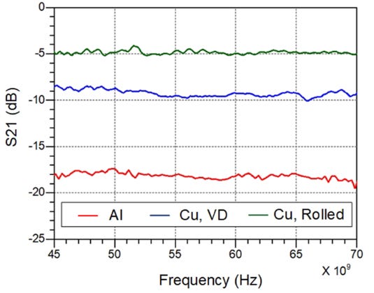
There are several claims online that this cable is immune to skin effect due to use of plastic as the waveguiding structure. This is simplistic and untrue. The authors of the paper show that the choice of aluminum versus copper, and even the surface roughness of the metal affects the attenuation per unit length from this interconnect. Skin depth and its associated losses does play a role, but likely not as much as in copper wires.
The choice of confining the field in the dielectric with just two plates, instead of enclosing it on all four sides like a rectangular waveguide, gives lower dispersion across frequency. Lower dispersion means that all frequencies have the same delay in getting to the other end of the interconnect.
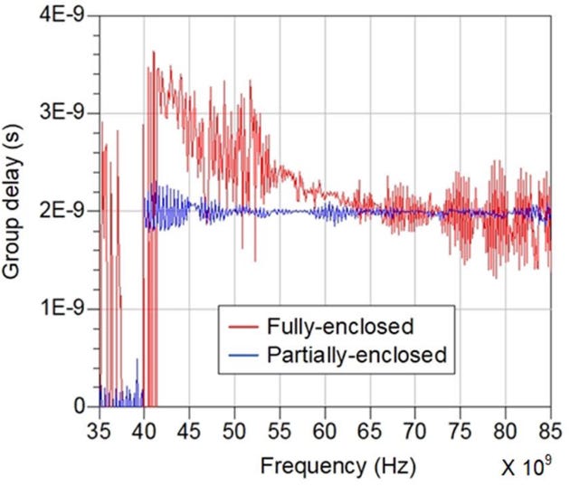
One of the stark benefits of using a parallel plate waveguide (in the 2020 paper) over using a circular cross-section tube (in the 2015 paper) is that its dominant electromagnetic propagation mode called Transverse Electromagnetic Mode (TEM) does not have a low frequency cut off. It transmits from DC to >100 GHz till higher order modes kick in. In other words, it acts just like a copper cable but with much lower loss. In contrast, a traditional rectangular waveguide with all four sides enclosed with metal has its TE10 dominant mode (TE11 for circular waveguide) only start propagating beyond its lower cutoff frequency, and acts more like a high pass filter. In this sense, the parallel plate waveguide is a better choice.
However, looking at the reported insertion loss performance of the interconnect shows that the bandwidth is limited between 50-70 GHz. Why?
My speculation is that the spectacular low-loss, broadband transmission property of TEM propagation in e-Tube is marred a major bottleneck: the microstrip-to-waveguide transition. This has implications on how this interconnect will scale to higher speed interconnects in the future.
After the paywall, for paid subscribers:
Microstrip to Waveguide Bottleneck: An in-depth look into the electromagnetics of the transition, and why it limits the performance of the interconnect.
Where CPO fits in: Why and how co-packaged optics is a competing technology to e-Tube.
e-Tube vs. AEC vs. CPO: A detailed discussion and comparison table based on power, speed, latency and reach, and where each technology shines.
Closing thoughts: A few odds and ends on what it would take for this technology to take center stage.