
Qualcomm's High Bandwidth Compute and the Packaging Problem It Moved
HBC stacking DRAM on the compute die increases memory bandwidth and skips CoWoS. The packaging problem does not go away, it shifts to 3D.

At its 2026 Investor Day, Qualcomm introduced High Bandwidth Compute (HBC), which is DRAM stacked on top of a logic die with a dense interface that gives high bandwidth between the two. It lays the foundation for Qualcomm’s route into the data center using a memory architecture that does not use the traditional HBM+CoWoS approach.
HBC is a platform technology, the foundation Qualcomm means to run through every business unit and not only the data center, and the whole thing rests on one move in packaging: it does not remove the hard part, it shifts it from the advanced substrate bracket (CoWoS) to a stacked-die approach that brings its own complexities.
Contents:
HBC as the Unit of AI Intelligence
Memory-on-Logic Packaging as a Key Risk Factor
Logic Die Function in HBM versus HBC
The Power Budget Under the Stack
Who Builds the HBC Stack
What to Watch For
Disclaimer: I am an ex-Qualcomm employee but hold no MNPI regarding their line of datacenter products. I worked as an RF engineer dealing with transistor devices – far from the sexy world of AI. The facts in this article are from public sources, and include my own inferences. I currently do not hold any QCOM stock. Not financial advice. Do your own research.
By reading this post, you agree to the terms and conditions. Also see the full ethics statement.
You can find the whole catalog of articles for purchase at this link. This article will be available for paid digital download shortly after publication.
If you would like to engage boutique research services for your project, reach out to us.
HBC as the Unit of AI Intelligence
The figure shows a standard packaging substrate with an System-on-Chip (SoC) and an low-power DDR (LPDDR) memory stack sitting on top of an XPU. At first glance it looks like an XPU next to HBM, but it is not that. The DRAM is stacked on the XPU, the die that runs the matrix multiplications, and the SoC beside it is a separate chip whose identity changes with the end market.
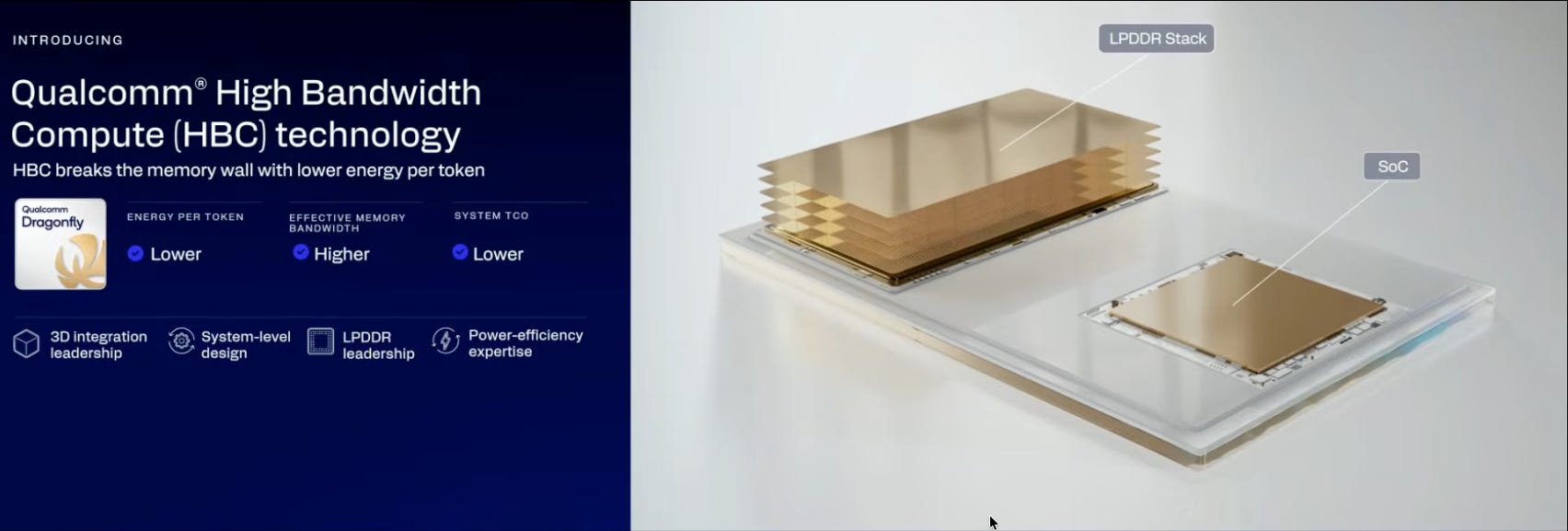
That second chip is the part Qualcomm has always built. It has been a modem, an automotive ADAS processor, an IoT SOC, and even a robotics chip. The XPU with the DRAM on top is the new part that provides Qualcomm with an AI accelerator. The main idea behind HBC for Qualcomm is for it to serve as the unit of intelligence, and pairing it with one of Qualcomm’s business-unit SoCs is what makes that line AI-enabled. As such, its applicability and importance extends to its entire business.
Memory-on-Logic Packaging as a Key Risk Factor
Qualcomm’s claim is that HBC removes the need for advanced packaging, whose supply chains are hard to get hold of right now, and that HBC therefore runs on standard packaging substrates, which are cheaper, more available, and easier to integrate on. HBC does avoid the 2.5D interposer that an XPU-plus-HBM design needs, and the gains it buys are real.
Stacking the memory on the logic die swaps the HBM path, a high-speed interface running along the die edge and out through an interposer, for short vertical links through the die area. That lifts the connection count from about 2,048 (in HBM4) along the edge to the order of 10,000-100,000 through the area, and it brings down the energy needed to move bits by an order of magnitude.
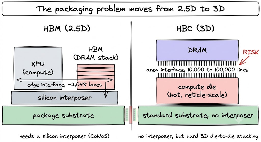
Qualcomm however glossed over the fact that packaging difficulty has not gone away. It moves from the advanced substrate (CoWoS) to 3D die-to-die stacking, which is also advanced packaging, and on a compute die, it is the harder version of it. Qualcomm is not removing the packaging step but instead trading a supply-constrained one for a harder and less proven one.
Stacking DRAM on logic is not new in itself. HBM already does it via a core logic die sitting under a stack of DRAM connected through silicon vias. HBC looks similar, but the logic die does a different job, and that difference is the whole risk.