
🍪 TWiC: MTIA x4, AVGO 400G, UMC, Nebius, SiPho Readiness++
This Week in Chips: Key developments across the semiconductor and adjacent universes.

Here is some content from this week in case you’ve been buried at work, and didn’t get a chance to look it over.
Substack: Why Optical Circuit Switching is Arista Networks’ Long-Term Problem
Semi Doped Podcast: The Great Optics-Copper Crossroads
Let’s get to the news. Lots of exciting stuff.
META: Four MTIA Chips in Two Years
Meta recently announced four Meta Training and Inference Accelerator (MTIA) chips that they are already using in deployment, or will roll out within the 2026-27 timeframe. These are chips developed in partnership with Broadcom (their custom accelerator business is looking pretty good), and is part of Meta’s strategy to vertically integrate their chip technology without relying on external supply from Nvidia, which allows them to save on infrastructure spend. Here is a quick rundown of what each chip is.
MTIA 300: Used already in ranking and recommendation (R&R) → 1 compute chips, 2 network chips, HBM stacks
MTIA 400: Next gen R&R chip + GenAI → 2 compute chips, 2 network chips, 1 PCIe chiplet, more HBM stacks and bandwidth
MTIA 450: GenAI optimized → 2 compute chips but faster, 2 network chips, 1 PCIe chiplet, 2x HBM bandwidth over MTIA 400
MTIA 500: GenAI beast → 4 compute chips (in 2x2), 2 network chips, 1 PCIe chiplet, more HBM capacity, 50% faster HBM bandwidth over MTIA 450
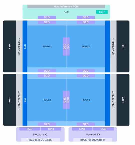
Meta’s approach to AI hardware is to build systems composed of smaller parts, like chiplets, that can be individually upgraded in quick succession as model architectures and numeric formats evolve. Meta is clear that they are adopting an “inference-first” approach to meet the growing GenAI inference demand.
Finally, MTIA uses a PyTorch-native approach to programming models which is a way of saying that models running on Nvidia hardware (using PyTorch on top of CUDA) can easily be ported over to MTIA with no rewriting. This allows Nvidia and MTIA hardware to work alongside each other with minimal friction.
(via Meta)
AVGO: Broadcom delivers Industry’s First 400G/lane Optical DSP for Next-Generation AI Networks
The Taurus BCM83640 is a 400G/lane optical DSP that builds towards 3.2T networking technology, especially when the TomaHawk 7 chip with 204.8 Tbps switch bandwidth is released. I particularly like the figure below that explains how 400G/lane is useful with both 1.6T and 3.2T optical technology.
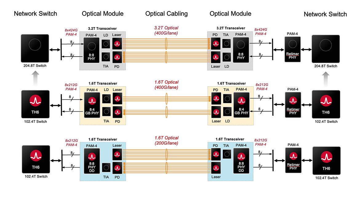
With the 1.6T generation, the optical DSP has a 8-lane to 4-lane gearbox that now only requires 4-lanes running at 400G/lane in a transceiver. With the transition to 3.2T, all 8 lanes run at 400G - no gearboxing required. According to Broadcom’s product page:
The BCM83640-DIE line (optical) transmitter supports multiple advanced 400G/lane laser optics, including a thin-film lithium niobate (TFLN) modulator, differential electro-absorption modulated lasers (D-EMLs), and advanced highbandwidth silicon photonics (SiPh) modulators.
It’s not clear to me why there is both a TFLN modulator and an electro-absorption modulator, but clearly TFLN’s high modulation bandwidth is very attractive in 400G networking. This DSP is built on TSMC 3nm and still uses IMDD for DR4 and FR4 reach. It is interesting to see when Coherent Lite will make an entry.
(via Broadcom)
UMC, HyperLight Team up to Mass-Produce TFLN Chiplets, Targeting 1.6T Data Center Bandwidth
Thin Film Lithium Niobate (TFLN) is going to become increasingly important for 1.6T networking generations and beyond because of the extreme modulation bandwidths possible. While the best InP EMLs for 200G/lane have a bandwidth of 60-67 GHz, TFLN modulators from Hyperlight exceed 110GHz. This is important for 400G/lane modulators, and is the same reason Broadcom’s recently announced 400G optical DSP uses TFLN (and D-EML?).
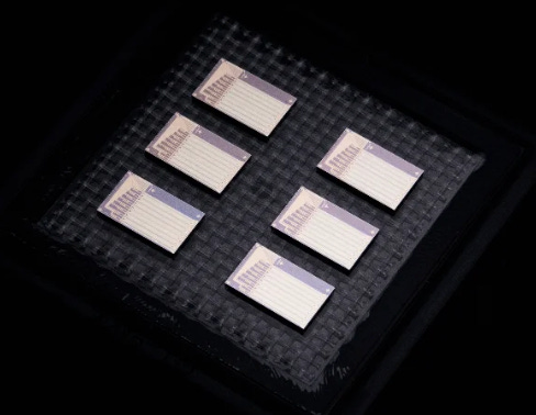
Hyperlight has a long standing relationship with Wavetek, and has ramped up HVM production of TFLN on 6” wafers. Wavetek is a fully owned subsidiary of United Microelectronics Corporation (UMC) - a major pure play silicon foundry. With parent company UMC getting into the mix, they are now looking to scale production to 8” wafers. In contrast, InP is still stuck on 3” and all talk of 6” wafers leads directly to supposed yield problems. TFLN on 8” sounds pretty good, and if yields/cost is good, are they a potential candidate for 200G applications in the face of InP shortages? Maybe some optics experts can weigh in, in the comments section.
(via TrendForce)
NVIDIA and Nebius partner to scale full-stack AI cloud
From the press release:
NVIDIA will invest $2 billion in Nebius, reflecting NVIDIA’s confidence in Nebius’s business and unique depth of engineering expertise across the full AI technology stack.
To enable Nebius to deploy more than 5 gigawatts of capacity by end of 2030, NVIDIA will support Nebius’s early adoption of the latest generation of NVIDIA’s accelerated computing platform.
The industry sentiment around this is generally positive because it provides Nebius early access to Vera Rubin hardware, additional cash flow and a positive endorsement from Nvidia whose $2B investment signals that they believe in Nebius’ future as an AI infrastructure provider. This is line with other investments Nvidia has made with Lumentum, Coherent, and CoreWeave recently.
The circular nature of deals made is a concern to many investors: Nvidia invests in Nebius, Nebius buys Nvidia hardware. The other point of concern is the growing debt Nebius is taking on — from nearly zero debt in 2024, to a total liability of $5.3B by the end of 2025. Nvidia’s $2B will help offset this, but the concern is that debt will grow as Nebius builds out towards 5GW of capacity.
(via Nebius)
Ayar Labs CEO Mark Wade: “Mass production of SiPh still faces many challenges”
In a DigiTimes exclusive interview, Ayar Labs CEO Mark Wade stated that the silicon photonics as a technology is ready, but mass producing it at scale is a difficult problem. I particularly like Wade’s response when asked what he thinks of the transition to optical in light of Hock Tan’s comments that copper is still relevant (emphasis mine):
SerDes and electronic transmission remain the dominant technologies today. Considering that many companies must comment on developments over the next few quarters, their statements are understandable. Our focus, however, is on what will happen in 2028, 2029, and 2030.
The SiPh supply chain’s mass production capability is currently not fully ready. But the pace of improvement in manufacturing readiness is accelerating. Together with our partners, we are actively ensuring the supply chain gradually comes into place to achieve our production targets.
I also agree that we will not wake up one day to find copper interconnects have completely disappeared. The transition will be gradual. Around 2028, GPUs and accelerators will begin adopting optical interconnects, and more AI infrastructure will rapidly shift toward optical communications. Statements from companies like Broadcom or Nvidia about copper remaining in use simply highlight that mass production of SiPh still faces many challenges.
(via DigiTimes)
eXtra-Dense Pluggable Optics (XPO): Liquid Cooled Insanity
A single sentence on Arista’s blog caught my attention.
XPO density is a game changer. A single XPO module replaces 8 OSFP modules.
")
The 8 OSFP connectors you see on the right are pluggables that go into ports in the optical switch. Now, the XPO module form factor provides 12.8 Tbps in a single plug, and it needs liquid cooling too. If you need a better introduction to what all the optical terminology means, check out my earlier post.
Arista goes on to explain the benefit XPO brings quite nicely.
In short, XPO allows customers to build large AI data centers with one quarter the switch racks. This is hugely important for both scale-up and scale-out applications, where without XPO the number of traditional switch racks would exceed the number of GPU racks.
Imagine a 400 MW AI datacenter with 1024 GPU racks of 128 GPUs each for a total of 128,000 GPUs. Assume 12.8T scale-up and 1.6T scale-out bandwidth per GPU. With OSFP switch racks that have a density of 1.6 Pbps per rack, this would require more than 1400 switch racks for scale-up and scale-out fabrics. With XPO, this would require 75% fewer racks, saving over 1050 racks or 44 % of the floor space.
More speed, fewer racks is good. Pretty sure you’ll see this at their OFC booth if you happen to stop by.
(via Arista blog)
Have a great weekend! NVIDIA GTC and OFC 2026 are both next week. Prepare for an explosion of new information! 💥
Avgo beat mrvl to the punch.