
Why is High Bandwidth Memory so Hard to Manufacture?
An in-depth look into the incredible engineering behind the memory used in GPUs for AI accelerators.

Welcome to a 🔒 subscriber-only deep-dive edition 🔒 of my weekly newsletter. Each week, I help investors, professionals and students stay up-to-date on complex topics, and navigate the semiconductor industry.
If you’re new, start here. As a paid subscriber, you will get additional in-depth content. We also have student discounts and lower annual pricing for purchasing power parity (see discounts). See here for all the benefits of upgrading your subscription tier!
High Bandwidth Memory (HBM) is the most critical component in AI hardware today.
GPUs can provide plenty of TFLOPS but modern compute has hit the ‘memory wall’ where compute resources stay idle while waiting for data from memory. Memory should have enough capacity to hold large model weights and sufficient bandwidth to transfer them quickly to the compute die when needed.
HBM is the only technology that can meet the memory demands for AI training, for now. This makes it a premium commodity.
HBM accounts for 50-60% of GPU manufacturing cost even considering that GPUs are made on leading edge silicon whose cost per wafer is well over $10,000. The estimated cost of HBM memory is $20-$100/GB (depending on pricing deals) when other memory technologies such as LPDDR and GDDR are under the $10/GB mark.
This top-shelf memory commands a premium price due to market demand of course, but more importantly due to the manufacturing complexity involved. There are only three major HBM manufacturers today: SK Hynix, Micron and Samsung. SK Hynix dominates 60-70% of the market share. Samsung has had its fair share of yield struggles in staying competitive in HBM. Another Chinese competitor, ChangXin Memory Technologies (CXMT), is quickly catching up in HBM playing field.
In this post, we will discuss why HBM is so hard to manufacture.
For free subscribers:
Fundamentals: The absolute basics of HBM and where it is used in a GPU.
Physical construction: How ultra-thin DRAM dies are stacked on a silicon interposer, and then placed on a substrate.
DRAM scaling: Fundamentals of DRAM including the 1T1C cell, implementation of capacitor structures, transition to 4F2 layout and vertical channel transistors, and 3D DRAM.
For paid subscribers:
Through Silicon Vias (TSVs): How they place constraints for HBM density, and how they are optimized for manufacturability and performance.
Yield, testing and repair: Difficulty of getting high yield, testing strategies needed, built-in self test and repair.
Bonding technologies: Detailed process flows for bonding using thermal compression and using mass reflow, comparison between TC-NCF and MR-MUF, and the future of hybrid bonding for HBM.
Read time: 15-20 mins
This post is too long for email. Please read it on Substack by clicking on the title.
Fundamentals
Let’s start with a 3D model of DRAM from SK Hynix that was on the exhibit floor of the 2025 TSMC Technology Symposium. The layered structure on the right is HBM, connected to an xPU (GPU/CPU) on the left through a silicon interposer. The interposer sits on a package substrate that often has more than sixteen layers and is built on Ajinomoto Buildup Film (ABF).

HBM has become an essential part of the AI revolution because a large number of weights need to be stored and accessed quickly by the GPU for training and inference. HBM is not particularly fast, but what it lacks in speed, it makes up for in capacity and bandwidth. It can store a large amount of data that can be accessed at a high bitrate.

The high data bandwidth comes from many parallel connections between HBM and the xPU. For HBM3, this means 1,024 parallel bits, and for HBM4 it increases to 2,048. To minimize latency, HBM is placed right next to the compute silicon. The shortage of chip real estate around the compute die, known as the shoreline, creates a physical limit on how much HBM can be placed around the chip. As models grow larger, this has led to the memory wall, where memory cannot provide data fast enough for computation tasks, either because of capacity limits or bandwidth.
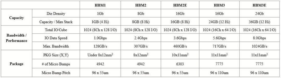
Let’s look at HBM3e closely in this table. Each DRAM die in the stack provides 3 GB capacity, and for a 12-hi stack, the total capacity is 36 GB. The data speed per pin is 8 Gbps or 1 GB/s and with 1,024 parallel IO lanes, its total data transfer rate is 1,024 GB/s. HBM4 will double the number of IO pins and increase the data rate to 1.5 GB/s, resulting in 3 TB/s bandwidth and up to 64 GB of capacity with a 16-hi stack.
Next, we will look at how the physical construction of HBM enables this incredible performance.
Physical Construction of HBM
HBM is built by stacking several DRAM die in 3D. Each DRAM die is a large array of memory cells made up of capacitors to hold charge and transistors that turn on and off to charge and discharge the capacitor. Later, we will look at the different ways these transistors and capacitors can be implemented in more detail.
Unlike logic, which is named by transistor gate length (7 nm, 5 nm, 3 nm, and so on), DRAM uses a different system based on the half-pitch of the memory cell. Half-pitch is half the center-to-center distance of the repeating memory structures on DRAM. DRAM nodes are labeled as 1x, 1y, 1z, with each letter marking a newer generation. More recently, Micron and SK Hynix have moved to 1𝛼, 1β, 1𝛄 nodes (or 1a, 1b, 1c in Samsung’s notation). There is no standard naming system, and the same node does not mean the same thing across different manufacturers.

Each die is between 30–50 µm thick, and HBM commonly stacks 4, 8, or 12 dies together (the topmost die is often thicker). In newer generations such as HBM4, the stack increases to 16 dies. The JEDEC specification limits total stack height to 720 µm for HBM3 and earlier, and to 775 µm for newer generations. This is about the thickness of an unprocessed silicon wafer, and the height limits exist because manufacturing processes are not designed to handle taller stacks.
The dies are connected with through-silicon vias (TSVs), which are 3D metal interconnections running through the die thickness, and microbumps with 30-50 µm pitch. All of the dies are then bonded together. At the bottom of the stack sits a unique logic die whose role is to handle read and write operations for the DRAM stack and manage data exchange with the external world. We won’t get into the details of logic die implementation in this post.
DRAM Scaling
It is remarkable that DRAM is more relevant than ever, considering its heyday was in the late 1980s when Japan dominated the market. DRAM has long since fallen off Moore’s law. A twofold increase in memory density now takes well over a decade. Structurally, a DRAM memory cell consists of a transistor and a capacitor, known as the 1T1C cell, invented by Robert Dennard (of Dennard scaling fame) in the early 1970s.
1T1C Cell
A single memory cell consists of a transistor and capacitor in series. When the transistor is turned on, the capacitor is charged. It will eventually discharge unless the cell is ‘refreshed’ within about 30-50 milliseconds. This is why it is called ‘dynamic’—because this kind of RAM does not hold charge when powered off.
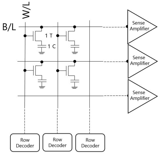
These 1T1C memory cells are arranged in an array, and each one can be accessed by applying a voltage to the correct row (called the bitline) and column (called the wordline). The stored charge is read out with the help of a sense amplifier, which boosts the output signal to a readable level. Both the 1T1C cell and the sense amplifier are central to DRAM operation and determine how its density scales.
Transistor, Capacitor and Sense Amplifier
One way to shrink the size of the memory cell is to use a smaller transistor. Moving to a more advanced node has no benefit if capacitor size remains the limiting factor. This is why DRAM chips today use 10–15 nm class transistor technologies. The naming system evolved to represent these as 1x nm, 1y nm, and 1z nm. For future generations of DRAM, EUV lithography becomes inevitable especially as gate lengths reach the 10 nm mark. For example, SK Hynix is already using EUV for its 1a nm DRAM node, and will continue to do so for future DRAM nodes. The roadmap below shows Micron’s use of different DRAM technologies, as another example.

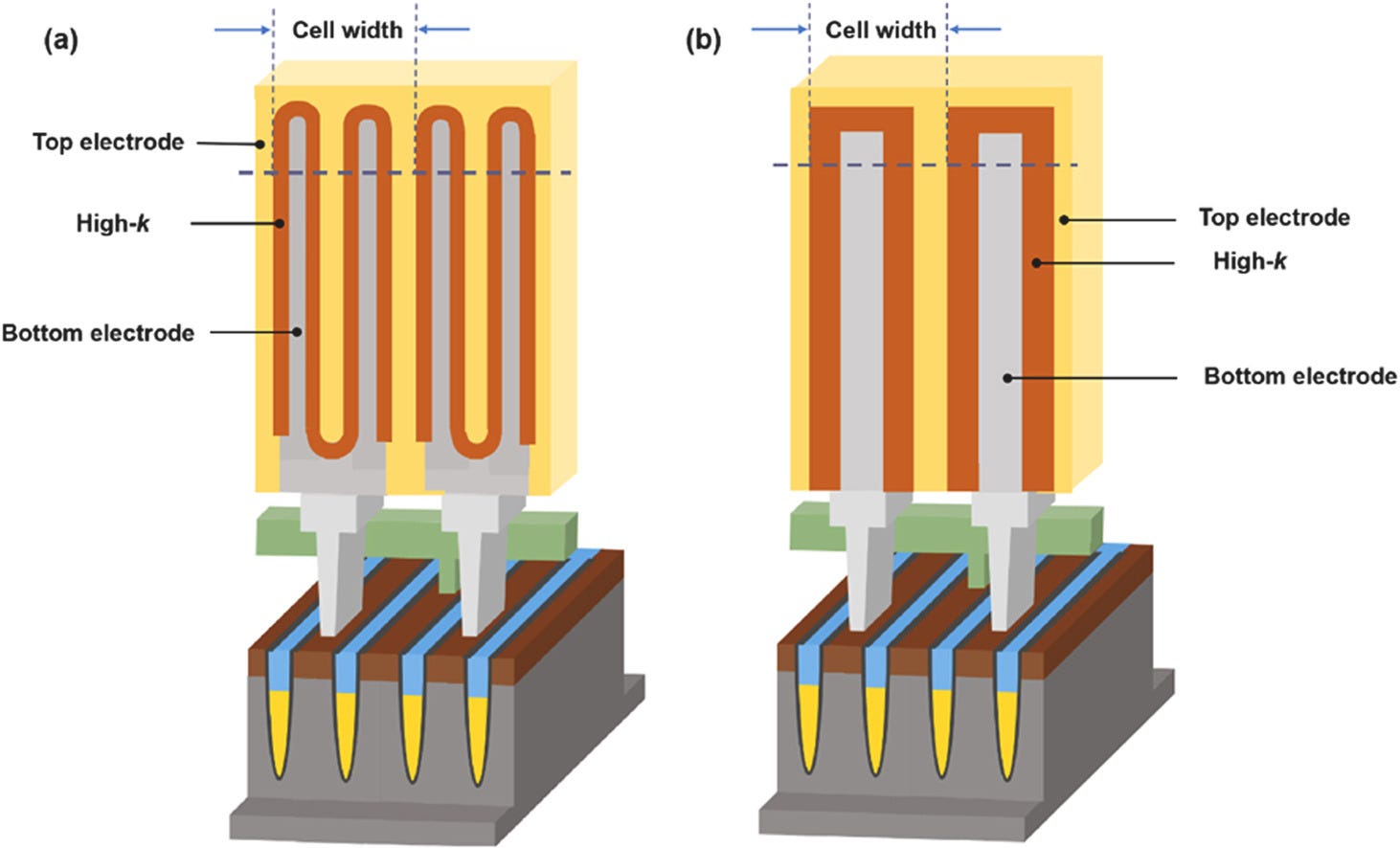
In the earliest implementations, the capacitor was planar and placed alongside the transistor. As technology evolved, capacitors were designed in new ways to reduce their footprint within the memory cell. Two forms have become widely used: trench and stacked. Trench capacitors are vertical structures built into the silicon substrate, while stacked capacitors are formed above the transistor.
Today, stacked capacitors are in mass production. They are either cylindrical structures, as shown in the left image below, or pillar-like structures, as in the one on the right. To maximize charge storage, the high-k dielectric between the electrodes is made very thin, often in the range of 5–10 nm. Below this thickness, charge leaks more quickly from the cell or reliability becomes a concern. The narrow structures used by these capacitors, with aspect ratios of 50:1 (500 µm high to 10 µm wide), make mass production difficult and further scaling increasingly challenging.
Lastly, the sense amplifier required at every bitline must also shrink along with memory cell sizes. As the transistors in the sense amplifier scale down, the use of lower drain voltages and greater transistor mismatch—a measure of how much two manufactured transistors can differ—makes it increasingly difficult to design low-power, accurate sense amplifiers for DRAM readout.
6F2 → 4F2: Vertical Channel Transistors (VCT)
In the late 1990s, each DRAM memory cell occupied an area of 4F × 2F = 8F², where F is the half-pitch of the memory cell, related to the combined size of the transistor and capacitor. Around 2004, Micron introduced the 6F² implementation of the unit cell by sharing active regions between neighboring memory cells. This resulted in a 25% improvement in bit density and significant efforts to bring the design into mass production.
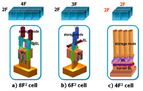
Interestingly, we are still using 6F² today, more than twenty years after its introduction. All DRAM improvements since then have come from optimizing capacitor structures and shrinking the transistor node at a slow pace. This has effectively stopped DRAM density from following Moore’s law.
The move to 4F² is still in the research phase and promises a 30% increase in bit density compared to what we have today. A 2F × 2F implementation requires memory cells to be stacked end-to-end at the minimum feature size, where 2F is twice the half-pitch and equal to the size of the memory cell. Achieving this requires a new transistor technology called Vertical Channel Transistors (VCT). Instead of using a planar transistor, the channel is rotated and built vertically to fit the full 1T1C structure within the minimum feature of the memory cell. Bringing this into production is a significant challenge.
3D DRAM
The future of DRAM becomes even more ambitious when it goes fully 3D, which is still in the research phase. This is not about stacking DRAM die as in HBM, or simply making the transistor vertical. It is about creating a true 3D implementation of the fundamental DRAM cell.
The concept of 3D DRAM starts with a 6F² cell that is laid on its side and stacked vertically to improve bit density. The higher the stack, the greater the density. Of course, this cannot be done literally because of lithography constraints. Instead, a 3D DRAM cell can be thought of as a 2D cell rotated on its side and built using gate-all-around (GAA) transistors, as shown below for a two-cell example.
 Move the bitline to the opposite side of the nanosheet; introduce Gate Forksheet design; reduce Active Area length, and change 2) introduce gate-all-around nanosheet transistors; introduce wider and shorter capacitances")
This can then be expanded to more than two cells as shown below.

This now forms the unit cell on any given layer, and can be stacked vertically from here on out. The picture below shows this for a 28-layer stack.

This approach is Lam Research’s vision for how 3D DRAM can be built. In reality, other approaches are also being explored, such as NEO Semiconductor’s X-DRAM cell designs, which promise a 10x improvement in DRAM density. Researchers at IMEC and Ghent University have already stacked 120 layers of 3D DRAM on a 300mm wafer.
Regardless of how complex it is to manufacture a single DRAM chip, packaging them vertically can make or break an HBM business. DRAM chips have been around for decades, but the real transformation lies in how DRAM is stacked to form HBM. We will look at this after the paywall.
For paid subscribers:
Through Silicon Vias (TSVs): How TSVs affect memory density and TSV optimizations.
Yield, testing and repair: Difficulty of getting high yield, pre- and post-stacking testing, yield and lifetime improvements by fixing defects with eFuses.
Bonding technologies: Comparison of MR-MUF and TC-NCF process flows and how SK Hynix and its unique material supplier hold market dominance, and the future of hybrid bonding for HBM.