

The 2025 International Electron Devices Meeting conference is a special one because it marks 100 years since the invention of the MOSFET by Julius Lilienfeld in 1925. The papers in the conference often deal with technologies far out from what is in production today but indicate where industry is heading. It is highly technical and is primarily aimed at people working on the cutting edge of technology.
Travel, stay, and per diem expenses are all covered with the help of paid subscriptions to this newsletter. I really appreciate your support. My special thanks to the IEDM publicity team for providing me conference access.
For free subscribers:
Qualcomm Keynote
Focus session on “Silicon Photonics for Energy Efficient AI Computing”
Tutorial sessions
Intel: Advances in CMOS Scaling and Future Challenges
TSMC: High-Speed Embedded Memory for AI Compute
For paid subscribers:
Short courses:
Samsung Research: Limitation and innovation of transistor technologies
IBM Research: Advanced Interconnect Technologies for Cu Extension and Beyond
Applied Materials: Process Technologies and Material Innovations to Sustain Moore’s Law in the era of hGAA and CFET
Univ. of Michigan: Silicon Photonics for High-Speed and Energy-Efficient Data Transfer
TSMC: Advanced Packaging and Chiplet Technologies for AI and HPC Applications
Notable technical sessions:
02-5: TSMC: CFET-based Ring Oscillators
16-3: CEA-LETI: SiGe HBT + RF-SOI on a Single Technology Platform
18-1: SK Hynix: Triple-Plug 321 Layer NAND Flash
18-5: SK Hynix: Multi-Site Cells for Penta-Level Cell NAND
36-2: Intel DrGaN: GaN Chiplets based on 300mm GaN-on-Silicon
You can purchase the full version of this post in epub formats supported by most e-readers using the button below.
For paid subscribers, the epub is available for download after the paywall, at the end of the post.
Keynote
There were three keynotes from Qualcomm, IBM, and GlobalFoundries. I’ll discuss Qualcomm’s keynote from PR “Chidi” Chidambaram, who is a Senior Vice President & Fellow at Qualcomm, because the talk was uniquely thought-provoking and liked by most for its technical depth for a keynote, which are otherwise generally marketing slides.
Disclosure: I am currently employed by Qualcomm, but opinions are still my own.
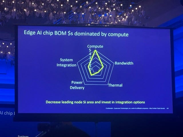
The talk was titled: “Electron Device Challenges to Enable Individual Centric Edge AI.” Running AI at the edge poses unique challenges related to how much compute and power is available. Apart from the obvious use cases of putting intelligence into edge devices like phones, laptops, and glasses, this talk showed that the biggest bill-of-materials cost in edge AI comes from compute.
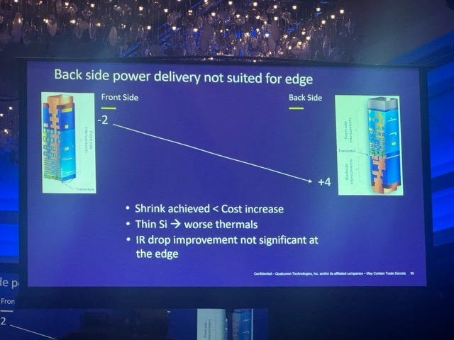
Chidambaram went on to say that back-side power delivery networks (BSPDNs) that are actively being developed for leading edge nodes by Intel and TSMC, are not well suited for edge applications. This is primarily because the silicon transistor where heat is generated goes in the middle of the dielectric stack, which makes it difficult to remove heat and manage thermals. Additionally, since edge devices will inherently run at lower power (and lower current), the IR drop improvement from using BSPDN is not significant. One could deal with the high resistance involved in supplying power through the frontside through all those narrow vias, and still get away with it. Source: Qualcomm.
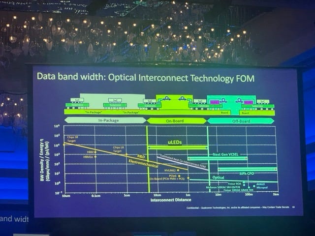
Finally, like in any talk about AI, there was a slide on interconnect bandwidth which had a surprising element on the slide - microLEDs! GaN-based LEDs for low power optical communication have been on the news cycles for a bit now, and especially with Credo’s acquisition of HyperLume. I thought it’s interesting that this was on a keynote slide given that there are currently no microLED-based active optical cables in deployment anywhere.
Focus Sessions
Some of the best talks of any conference are rear loaded at the end of the conference simply to ensure that attendees stick around long enough before partaking in the local scenery. IEDM was no exception. Focus session #4 titled “Silicon Photonics for Energy Efficient AI Computing” had quite the star-studded invited cast featuring Nvidia, Google, IMEC, DARPA, IBM and NTT. I did not attend other focus sessions although they seemed interesting. We will only discuss Nvidia and Google here because the others didn’t stand out to me as much.
Nvidia
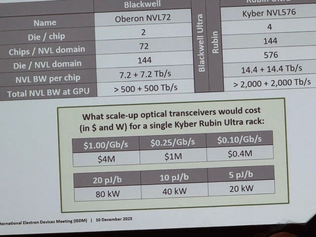
Nvidia’s talk was on “Photonic Interconnect for Next-Generation AI Systems” in which they firmly emphasized that optics was prohibitively expensive for rack scale up. They showed numbers to back that up based on what “hypothetical” scale-up optics would cost for a Kyber Rubin Ultra rack. The 5 pJ/b energy efficiency number is pretty much in line with CPO which uses 9W for 1.6 Tbps interconnect, or 5.6 pJ/b (from Nvidia’s slide in the same talk).
On the topic of CPO, Nvidia had some power calculations for various CPO implementations versus pluggable. CPO according to Nvidia has two flavors:
CPO over organic substrate or multi-chip module (MCM): Here the optical engine (OE) is on the substrate holding the interposer+switch silicon. Technically, this is not the closest possible location for the OE in relation to the switch ASIC.
CPO on interposer (or “aspirational” 2.5D optics): Here the OE is packaged as close as possible to the switch chip for minimal interconnect distance, and is ideally the way CPO should be implemented albeit at higher cost/complexity when packaging on the interposer. This involves putting the OE on the silicon interposer using CoWoS.
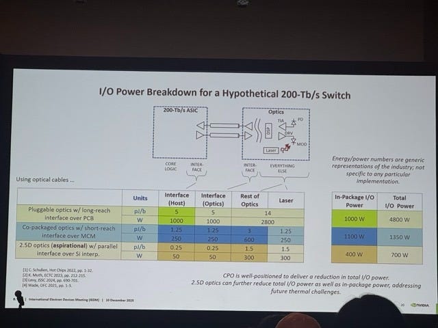
I like to look at pJ/b numbers for each of these three hypothetical 200 Tbps switch implementations (the fastest switch as of this writing is Broadcom’s Tomahawk 6 at 102.4 Tbps; we are really looking at next generation here):
Pluggable optics: Total energy efficiency = 24 pJ/bit, where the transceiver itself takes up half the energy budget at 14 pJ/bit.
CPO on MCM: Total energy efficiency = 6.75 pJ/bit. Optical transceiver does not need power hungry DSP, and this drops the overall energy usage.
CPO on interposer: Total energy efficiency = 3.5 pJ/bit. Because the OE is so close to the switch, the interface electronics get greatly simplified, and uses only 0.25 pJ/bit on each side. Note that the laser energy is slightly higher (1.5 pJ/b) compared to 1.25 pJ/b for CPO on MCM. This is because the optical signal from the faceplate needs to travel slightly longer to the interposer, and hence a higher power laser is needed.
Anyway, here is Nvidia’s concluding word on optical scale-up:
For scale up, the extended reach of optics can simplify thermal and mechanical design and enable larger domain sizes – but only if the power and cost of optics can be reduced.
Optics for scale-up is quite some ways away, so investors should not read too much into it just yet. I have a whole post discussing why active electrical cables (AEC) is here to stay for at least one more networking generation.

Google
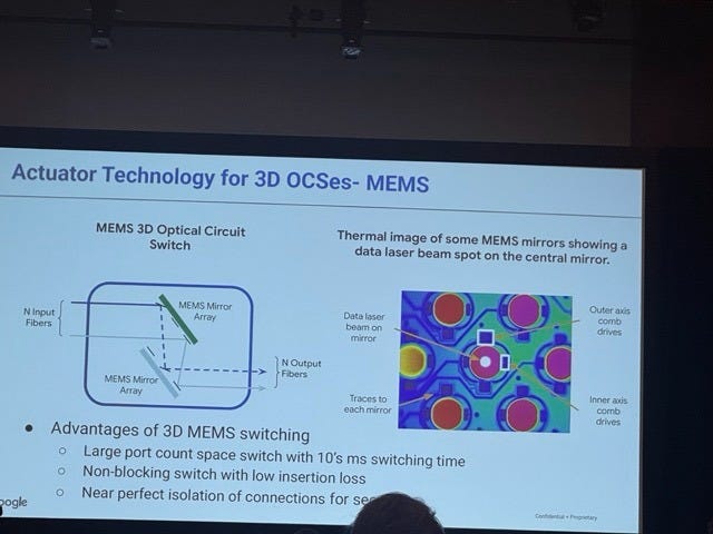
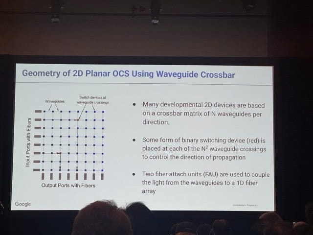
Google’s invited talk was titled “What’s Next for Optical Switching?” Ever since TPUs have come into the mainstream media since the launch of Gemini 3, optical circuit switches (OCSes) are more discussed than ever because these “purely light based” switches are instrumental in hooking up TPU pods together. Google has had their in-house MEMS OCS for a while now, and Lumentum was bullish about OCS in their recent earnings call.
OCS is simple in concept in its basic form. Imagine an optical signal coming from a source port on a switch, and you want to send it to a destination port. You simply put a tiny mirror and angle it just right - like using a hand mirror to reflect sunlight from a window onto a spot on the wall. The nice thing about mirrors is that they reflect all wavelengths of light, unlike the liquid crystal approach from Coherent which are wavelength dependent – and therefore require different SKUs per optical band.
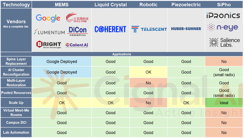
The table from Cignal AI below shows the different optical switching solutions in the market today.
Actually, I liked an OCS slide from a KAIST talk in the same session that put numbers in the right places, made good comparisons, and provided references. Here it is below.
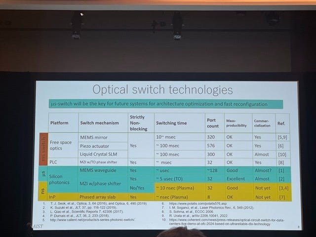
Making an integrated solution to optical switching using silicon photonics or other similar 2D approaches is something that’s still under development. Switches based on Mech-Zehnder Interferometers (MZIs) or MicroRing Modulators (MRRs) are possible on a 2D level by switching a cross-bar matrix of optical waveguides.
Tutorial Sessions
I like attending tutorials because they usually start from the basics, as opposed to technical sessions presenting the cutting edge. We’ll discuss two of them below.
1. Intel: Advances in CMOS Scaling and Future Challenges
This tutorial talk was an overview of how silicon technology has evolved from planar MOSFETs, to FinFets and gate-all-around (GAA) transistors, and what’s coming next. The proposed timeline looks something like this.
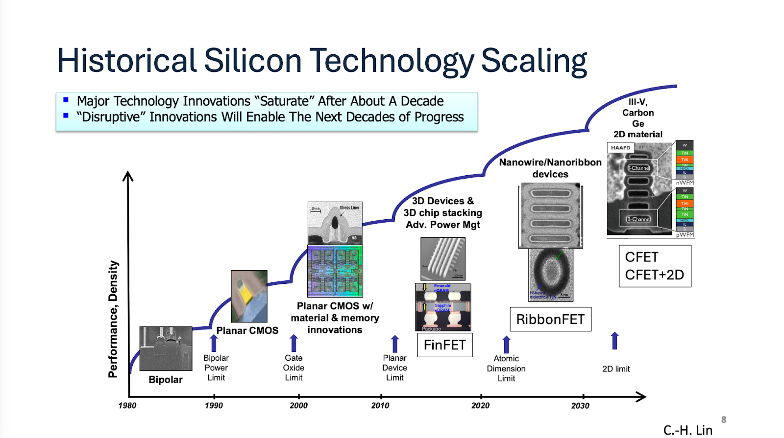
Planar FETs control the silicon channel where current flows from one side. A giant leap came in FinFETs, where the channel looked like a shark-fin and could be controlled from 3 sides. A gate-all-around FET (GAAFET, RibbonFET, Nanosheet FET, Forksheet are all slight variations) controls the conducting channel on all four sides, which provides the best control over turning the transistor on/off.
Transistors in the next decade would have GAA devices stacked on top of each other - like NMOS on top of PMOS to save space. In terms of node naming conventions, CFET would enable nodes below A7 or 0.7nm which is quite a ways out. CFETs can be made with three different flows:
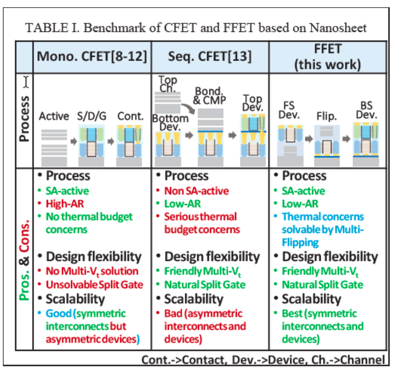
Monolithically: the NMOS and PMOS are made together in one flow.
Sequentially: The bottom PMOS is built first, then oxides are deposited and the top NMOS is built after that.
Flipped: The bottom PMOS is built, then flipped onto another silicon wafer, the wafer is ground back and then the NMOS is built. A senior process engineer I spoke to at a prominent foundry said that there are issues with this flipping approach that makes it challenging to take to market, but wouldn’t say why.
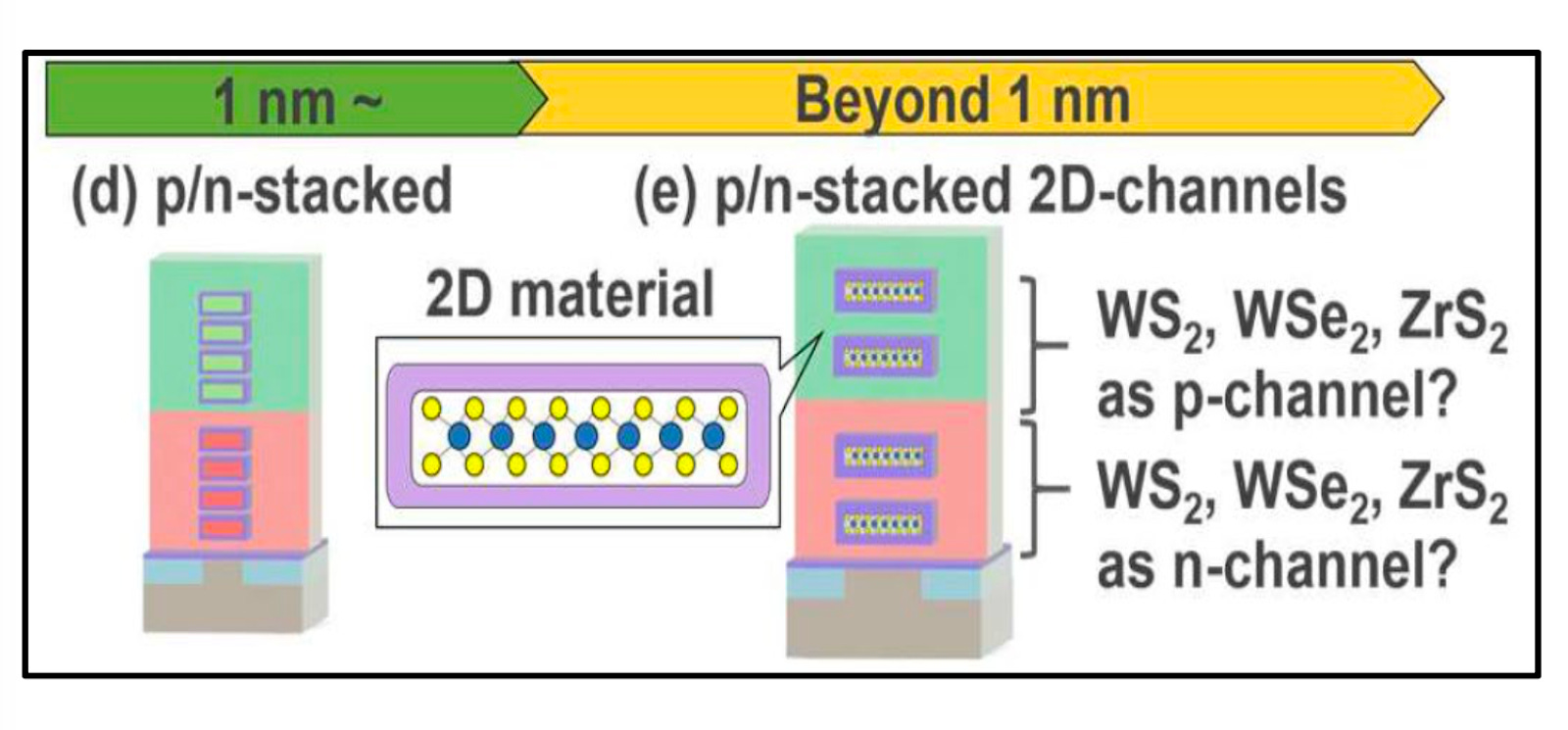
Ultimately, the CFET will use 2D materials like MoS2 to reduce the vertical height of the stacked transistor, but this is really far out into the future. These are materials like MoS2, WS2, WSe2, and others that are used instead of the silicon channel, but they are 1-2 atomic layers thick - almost 2D.
The base CFET is still not finalized in its base form. For example, someone asked a TSMC presenter why they put the PMOS below and NMOS on top. Although there are valid reasons this is currently the choice, the presenter said that nothing is set in stone and going forward, it could very well be swapped. Some of these developments are still far out and are works in progress.
2. TSMC: High-Speed Embedded Memory for AI Compute
Another highly discussed topic at the conference was the AI “memory wall” and there were many potential solutions being presented involving different kinds of memory and in-memory compute. I particularly liked this talk because it took the audience through a variety of topics without being overwhelming.
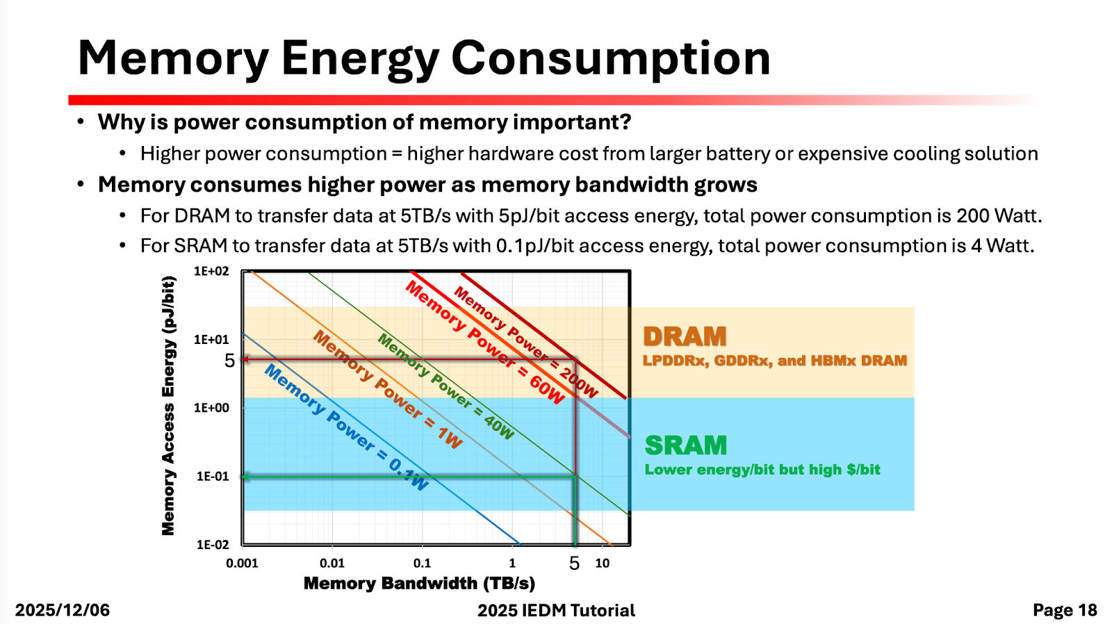
The speaker identified that any embedded memory used for AI can be evaluated on five different criteria: capacity, density, bandwidth, latency, and energy. Two popular memory choices for compute are always DRAM/HBM and SRAM, and I really liked the plot below that shows different frontiers of how energy and bandwidth are related (even more relevant given the current “SRAM for inference” dialogue).
The talk covered the basics of SRAM operation, device sizing tradeoffs, read and write assist techniques, and optimizing metal resistance and capacitance for better performance. It was all basic and understandable to anyone who hasn’t seen this stuff before. It provides a good start but you will still have to later explore this on your own.
One of the main reasons for the chart up above was so that we could talk about compute-in-memory architectures. After a brief but basic discussion on SRAM/DRAM, we suddenly found ourselves discussing magneto-resistive RAM (MRAM). The basic idea is that it uses a magnetic tunnelling junction (MTJ) that can be programmed to hold a 0 or 1 state. It looks like this:
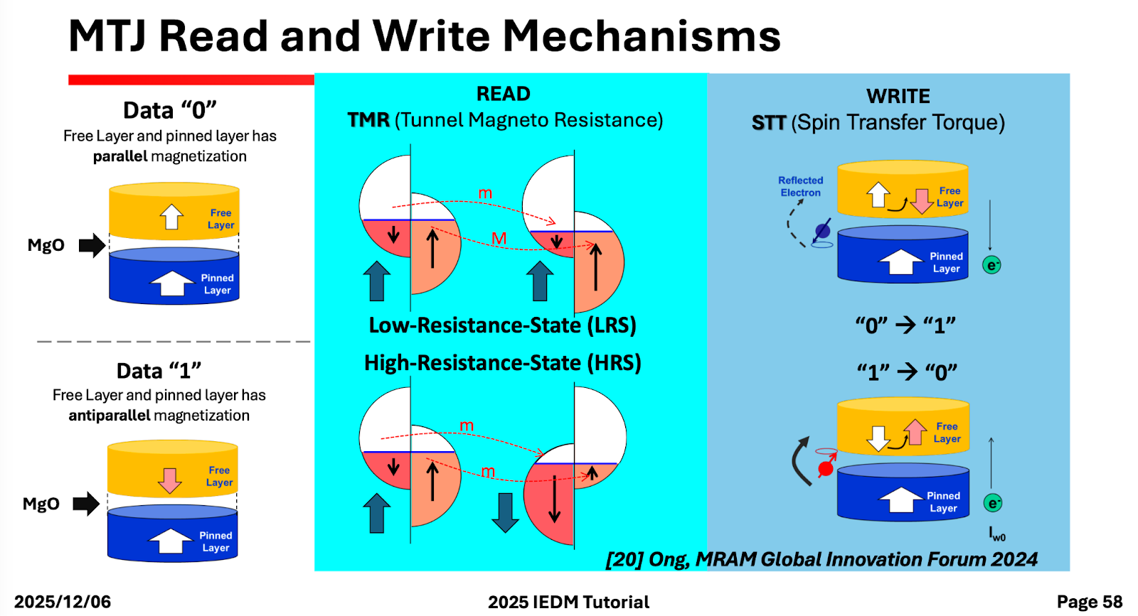
Depending on the magnetization of the free and pinned layers, the MTJ exhibits a low or high tunnel magneto-resistance. That’s about all I know about MTJs; I have to read and write a separate post if you want to know more.
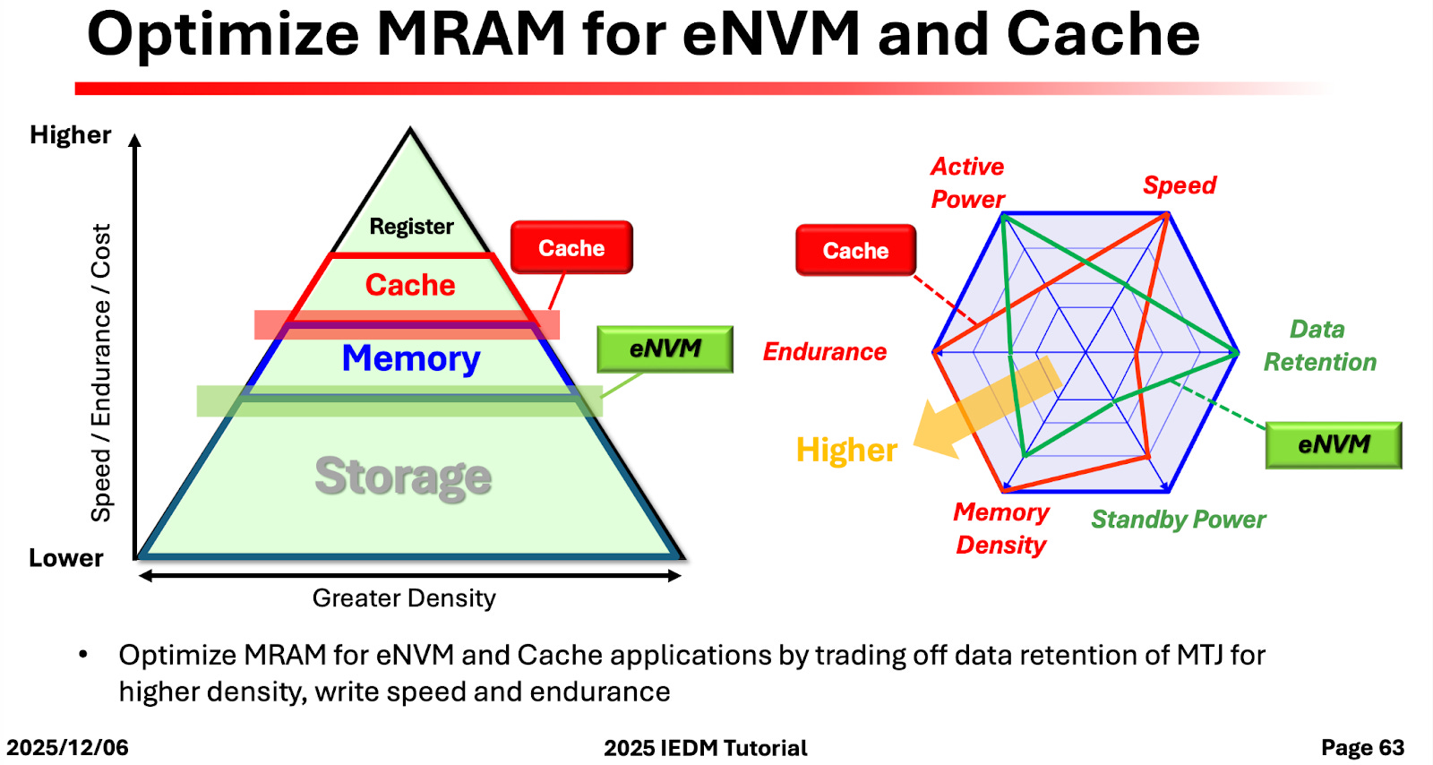
As it turns out, you can build the MTJ differently depending on what you want to use it for. In effect, you could design MTJ as non volatile memory like flash, or as volatile memory like DDR. Depending on the device design choices, MRAM occupies the region between cache and storage, interestingly lying in the same region that HBM lives. However, MRAM does not offer the kind of density that HBM does.
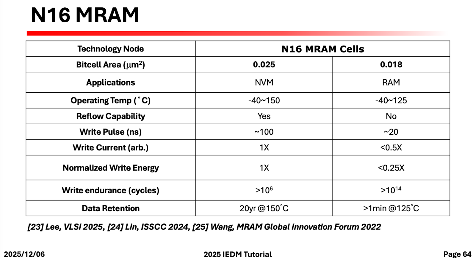
The most important thing for this kind of memory to work is that you have to keep real magnets away from it, at a distance of 1 cm at the very least. That can often be arranged in practice. There was a lot of discussion on MRAM in this conference, but I am not entirely sure how close it is to being practical.


