
A Close Look at SRAM for Inference in the Age of HBM Supremacy
Why SRAM for AI inference is far from the silver bullet everyone is expecting, an in-depth look into SRAM's specific performance benefits, and why HBM is here to stay.


The recent news of static RAM (SRAM) based accelerators has led to a flurry of discussion about memory on social media. It is uniquely attractive because it avoids the use of high bandwidth memory (HBM) and chip-on-wafer-on-substrate (CoWoS) packaging, both of which are heavily supply constrained.
However, there is a lot of misunderstanding on what SRAM actually is, and how it differs from the incumbent HBM solution. There are also misguided fears that SRAM will affect demand for HBM in future AI accelerators. Even Jensen Huang got asked about SRAM vs. HBM. I made a quick clarification on X about some basic SRAM facts that can help people cut through the noise, which became my most viral post ever.
In this article, we will discuss the pros and cons of SRAM compared to HBM and provide objective perspectives on the role of each kind of memory for AI inference. We will compare SRAM and HBM across five categories: structure, scaling, capacity, bandwidth, and cost.
For this piece, I am joined by Subbu who writes the Chip Log publication on Substack. He is an expert in memory interfaces for AI accelerators, and works for d-Matrix building their next generation Raptor inference architecture. Subscribe to his Substack for deep insights into chip design from someone who has worked in semiconductors for two decades.
Here is a post outline:
SRAM Overview
Unit Cell Structure: 6T SRAM vs 1T1C DRAM
Process and Density Scaling
Capacity
Bandwidth Performance
SRAM Scaling Limits
For paid subscribers:
SRAM vs. HBM cost comparisons
If you would like to purchase an ebook version of this post, use the button below. Paid subscribers get the same downloadable epub for free, after the paywall.
Note: This article has been updated since it was originally published and corrections have been propagated to all sources, including downloadable digital content. Here is the published errata.

SRAM Overview
SRAM is a form of memory often found in processors that holds digital information without the need for constant refreshing. Once a 0 or 1 is written to an SRAM unit cell, it holds its state as long as power is available, unless intentionally changed.
The use of SRAM in computing is as old as computers themselves. They are most commonly used in registers and low level caches often referred to as L1-L3 (L1 is closest, L3 is farthest) depending on how close to the processor it is located. The main attraction of SRAM is the blazing fast access speeds that feed data to a processor with absolute minimal latency. In fact, no other current memory technology can surpass the access speeds of SRAM - even HBM.
The ultra low latency and low energy usage of SRAM stems from the fact that this memory is located on-chip along with the processor. However, what you gain in SRAM performance is lost in the capacity it can store. The amount of SRAM you can place in one square millimeter of chip area is 5-6 times lower than dynamic RAM (DRAM). HBM vertically stacks 12-16 of these DRAM chips to further increase capacity. In effect, HBM easily has 80 times more capacity than SRAM.
Unlike HBM, SRAM is usually not manufactured separately and co-packaged with a GPU (exceptions exist). To fully realize the performance benefits of SRAM, it has to be on the same chip as the processor.
SRAM capacity can be increased by stacking SRAM chips on top of compute chips as was done by AMD in their 3D V-Cache technology. But there is no multi-stacked SRAM in production today, like DRAM is stacked 12-16 times to create HBM. Some interesting implementations in the past have disaggregated SRAM chips, and packaged them alongside HBM; but we’ll discuss those in a later post.
We’ll revisit a lot of these ideas with a focus on SRAM specifics in the coming sections. But first, if you need a primer on HBM, see an earlier post below that goes into this in quite some depth. It will be helpful when we make comparisons between SRAM and HBM in this post:

Unit Cell Structure: 6T SRAM vs 1T1C DRAM
To appreciate the real difference between SRAM and DRAM, it is important to understand their implementation with fundamental components, and how it ties into process technology.
6T SRAM
Each SRAM cell is commonly implemented in a six-transistor (6T) configuration as shown below. It consists of a four-transistor cross-coupled CMOS inverter called a ‘bi-stable latch’ that holds the cell state, and two NMOS access transistors used to read and write to the cell. This 6T SRAM structure is placed on a 2×2 grid - with control voltages applied to rows and columns to control the state of each cell. The gates of the access transistor are connected to the columns of the grid, also called bitlines (BL, BL’); the gates are connected to rows, also called wordlines (WL).
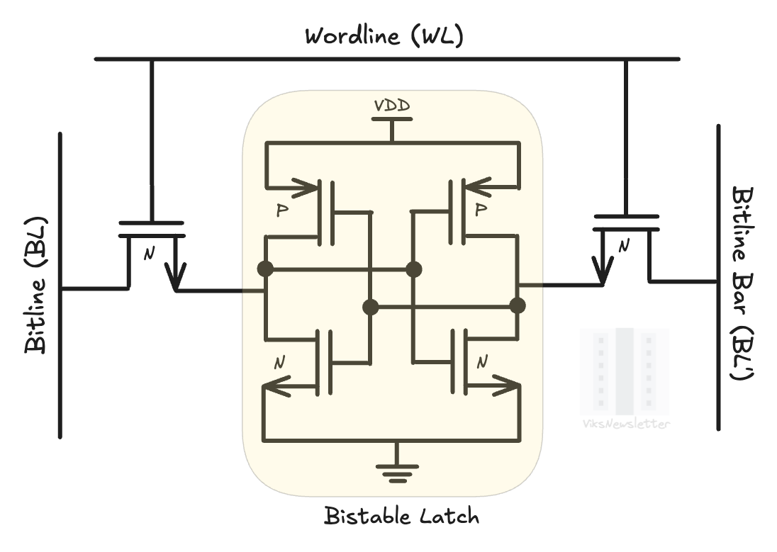
Three operations can be performed on this 6T unit cell: hold, read, and write. The picture below shows how each of these states are achieved with voltages on bitlines and wordlines.
Hold: WL is set low (for example, at 0 volts), which turns off access transistors. The inverters in the bistable latch hold their state of either 0 or 1 as long as Vdd is supplied.
Read: WL is set high (Vdd); BL and BL’ are set to Vdd. Depending on the internal bit stored, one of the access transistors will pull down BL or BL’ slightly depending on where a 0 or 1 is stored. A sense amplifier detects which bitline (BL or BL’) got pulled down, and determines the internal bit state.
Write: WL is set high; Then 0V or VDD is forced on BL (VDD or 0V on BL’) to set the internal bit state of the bi-stable latch at 0 or 1.
This is how the SRAM cell operates to store information without needing to constantly be refreshed to hold information like DRAM, and how bit values are read from and written to it.
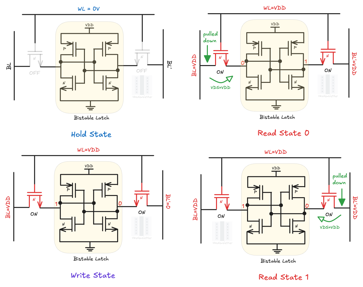
1T1C DRAM
The internal structure of a DRAM cell is far simpler than SRAM, and consists of a single transistor in series with a capacitor (1T1C). Its sheer simplicity with just two elements explains why more DRAM cells fit into a given area of a chip compared to the six transistors needed for SRAM.
The transistor is an n-type MOS device that acts as an access transistor to the capacitor. When the access transistor is turned on by applying a voltage to its gate via the wordline, the capacitor is charged up and the cell now represents a bit state of 1. The wordline voltage applied is typically higher than Vdd by the threshold voltage of the nMOS transistor. This ensures that the capacitor receives the full Vdd voltage for charging up.
When the wordline voltage is set low, or 0V, the access transistor turns off, and the capacitor is isolated from the bitline. Depending on whether the capacitor has charge or not, the DRAM cell represents a 1 or 0, respectively. However, the cell cannot remain in this state indefinitely. Charge eventually starts to leak out, and the cell must be refreshed to maintain its state; hence dynamic RAM.
Writing to a DRAM cell is straightforward. The wordline is set to a high voltage which turns on the access transistor. The bitline voltage is set to Vdd or 0 depending on whether the bit state is 1 or 0, respectively. After a few nanoseconds, the wordline is set to a low voltage trapping the charge in the capacitor.
In the simplest case, reading from a DRAM cell involves first precharging the bitline to Vdd/2. Then, when the wordline is activated to turn on the transistor, the bitline voltage will pull higher than Vdd/2 if the capacitor was charged (storing bit 1), or will pull lower than Vdd/2 if the capacitor was discharged (storing bit 0). These voltage differences are detected using a sensing amplifier to detect the bit state. In practice, DRAM sensing is a fair bit more complicated, but this should give a basic understanding of how it works.
Process and Density Scaling
SRAM
While the design tradeoffs and techniques in the 6T unit cell can get quite involved, here is a key takeaway: if the transistors can be made smaller, we can pack more of them to improve memory density.
In the early days of planar transistors, every generation of smaller transistors led to higher SRAM memory density. This was true until Dennard scaling ended, and subthreshold leakage got worse with every smaller transistor generation. Subthreshold leakage is a term that signifies how much current the transistor leaks when it is off - something it is ideally not supposed to be doing. Additionally, smaller transistors had a lot of variability that led to the bi-stable latch accidentally flipping its bit state, causing bit errors.
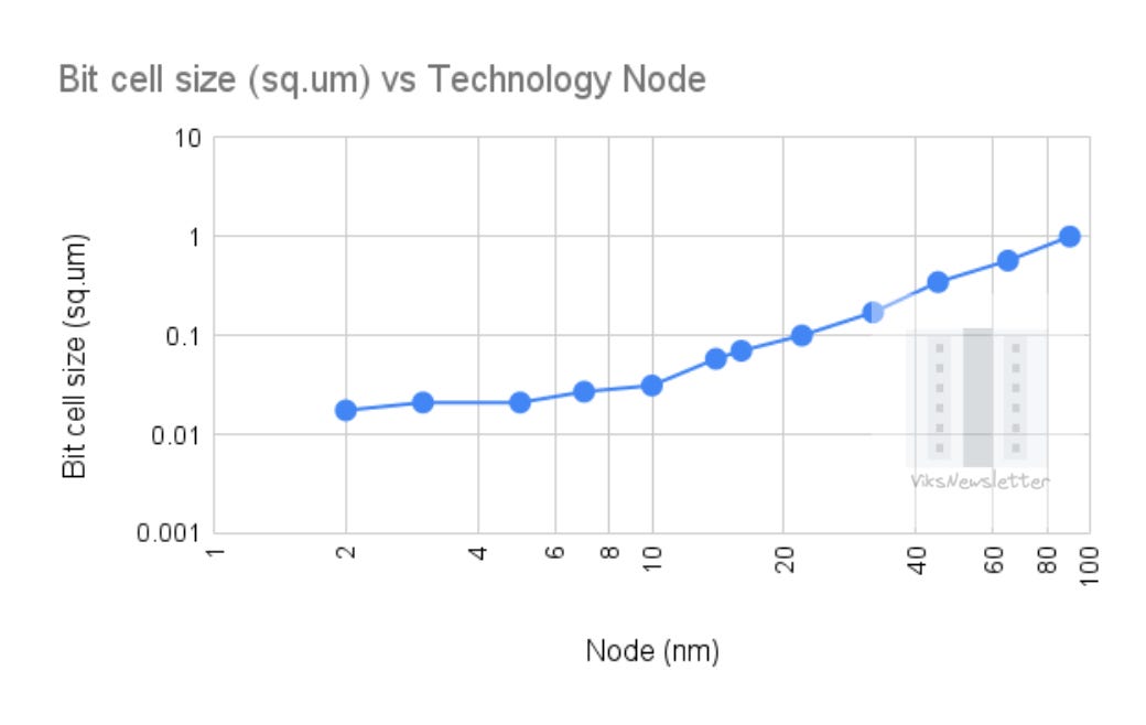
The move to FinFETs around the 14nm node meant that transistors were both smaller, and had better control over the silicon channel which enabled some more SRAM scaling. However, right around the 5-7nm node, SRAM scaling seemed to flatten out. This became evident when TSMC’s N3E had the same bitcell size as N5 (0.021 sq. microns).
The move to gate-all-around transistors in TSMC N2 provided the first SRAM scaling since N5, where the bit cell size went to 0.0175 sq. microns: a ~17% shrink. Intel’s 18A results at the 2025 ISSCC still showed a 0.021 sq. microns bit size; not a significant shrink.
In essence, we have reached the limit of what is possible with our current technology capability with regards to SRAM. The days of SRAM density doubling every two years is well behind us. The best memory density we can get today is about 38 Mb/mm2 with SRAM.
There is some possibility of further SRAM scaling when we get to complementary FETs (CFETs) where the NMOS is stacked on PMOS. The bi-stable latch has two inverters that will get smaller with CFETs. Radical alternatives are being looked at with magnetoresistive RAM (MRAM) and ferroelectric RAM (FeRAM) that might provide us with a much needed breakthrough at scale.
DRAM
The 1T1C cell used in DRAM is uniquely engineered to maximize memory density. DRAM chips are built on specialized chip processes specifically designed for memory, and go by the names 1a, 1b, 1c, which is different from how advanced logic nodes used for SRAM are named (5nm, 3nm, 2nm).
Memory process nodes stack the capacitor on top of the transistor using a high aspect ratio capacitor structure that often uses high-k dielectrics like hafnium or zirconium oxide to maximize capacitance and minimize leakage. The access transistors are the equivalent of a 10nm logic transistor or higher because the limiting factor for unit-cell size is the capacitor, not the transistor. Going to smaller channel transistors would increase both leakage and cost.
DRAM has its challenges in scaling memory density too. For the last 20 years, the size of a DRAM cell has been stuck at 6F2, where F is the half-pitch of the memory cell. Increasing DRAM density requires shrinking the capacitor and transistor to reduce F, and slow progress has been made over the years on this front because there is little that can be done via lithography to make things significantly smaller.
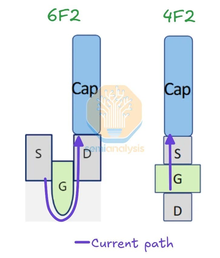
The next quantum leap will come when we go to a 4F2 unit cell structure, which implies that the memory cells are stacked back-to-back with no space between them. This requires a vertical channel transistor possibly with the use of Indium Gallium Zinc Oxide (IGZO) channels and a true 3D DRAM unit cell that is actively being pursued by startups such as Neo Semiconductor.
Capacity
In general, when it comes to capacity, all DRAM technologies whether HBM, LPDDR, or GDDR have an advantage over SRAM. The fundamental difference in their cell structure, as we saw above, directly affects how much memory can be packed into a given die area. With HBM3e, density is on the order of ~200 Mb of DRAM per mm², while at TSMC’s N3E node, 1 mm² of silicon can hold only ~38 Mb of SRAM.
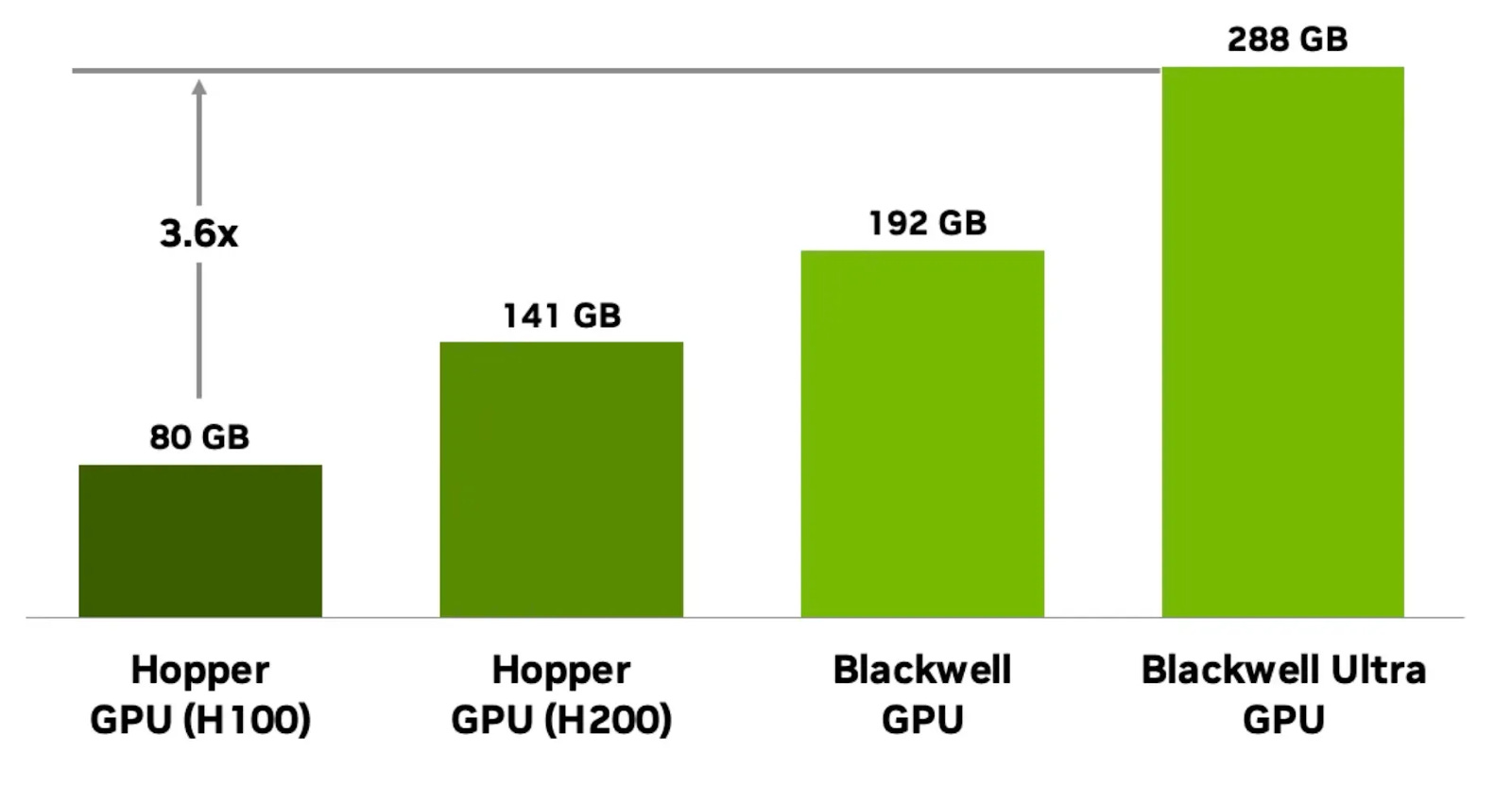
HBM also benefits from vertical stacking. Each of the DRAM dies in a HBM3e stack is 11mm x 11mm in area and has a capacity of 3GB (24Gb) at present. A GPU like Blackwell Ultra uses eight 12-high HBM3e stacks, adding up to 288 GB of total memory (12-Hi × 3 GB × 8 stacks).
In contrast, SRAM competes directly with compute and other on-die resources for die area. Every additional megabyte of SRAM comes at the expense of compute units, interconnect, or control logic, making its size a constant trade-off. As a result, even on large accelerators, on-die SRAM is typically limited to at most a few hundred megabytes per chiplet.
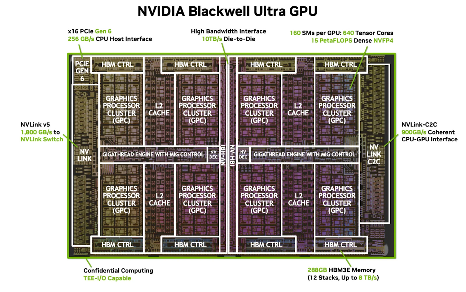
Below is a die-shot of the Blackwell Ultra GPU, showing its composition and the various blocks that contend for the die area. The L2 cache is built with SRAM, and making it any larger will come at the cost of smaller graphics processor clusters and lower total compute flops.
Effects of capacity on model parallelism
Modern LLMs are large enough that they often need to be sharded across multiple GPUs or XPUs even when HBM is available because the memory requirements exceed what is available on a single GPU. Two common ways to do this are tensor parallelism and pipeline parallelism, which differ in how the model is split across devices. The figure below illustrates both approaches.
Tensor parallelism (intra-layer parallelism) splits the matrix multiplications within a single layer across multiple GPUs, while pipeline parallelism (inter-layer parallelism) divides transformer layers themselves across multiple GPUs.
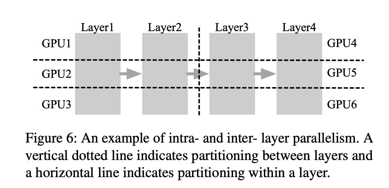
In practice, these strategies are usually combined. For example, a LLaMA-405B model, which has 126 layers, might be spread across two DGX-H100 nodes, each with eight H100 GPUs. Within each node, tensor parallelism is used, while pipeline parallelism connects the two nodes.
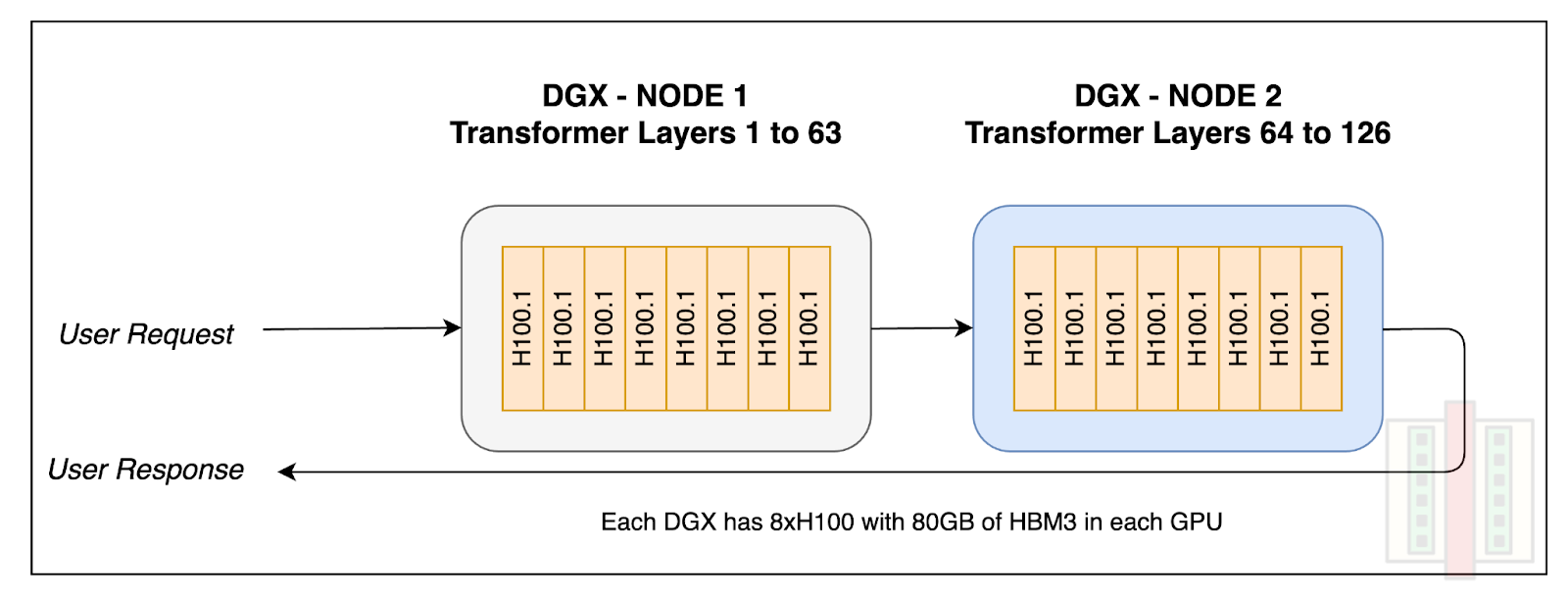
On SRAM-based accelerators, the same models would typically be distributed across a larger number of chips due to limitations in available memory per chip. This places more responsibility on the compiler and runtime to efficiently partition and coordinate work across devices, and as a result becomes increasingly complex and inefficient to orchestrate. Designing these systems well is definitely possible, but it adds complexity and requires careful orchestration to avoid efficiency losses.
Bandwidth Performance
Memory bandwidth equals the width of the memory interface multiplied by the data transfer rate. For any memory system, you can increase bandwidth by making the interface wider (more parallel data paths), running it faster, or both. With regard to bandwidth, there are 3 factors that make SRAM better than DRAMs.
1. SRAM bandwidth is an order of magnitude higher than HBM
Take the NVIDIA B200 as an example:
Each stack of HBM3e provides ~1 TB/s. With 8 stacks, that’s 8 TB/s of peak DRAM bandwidth.
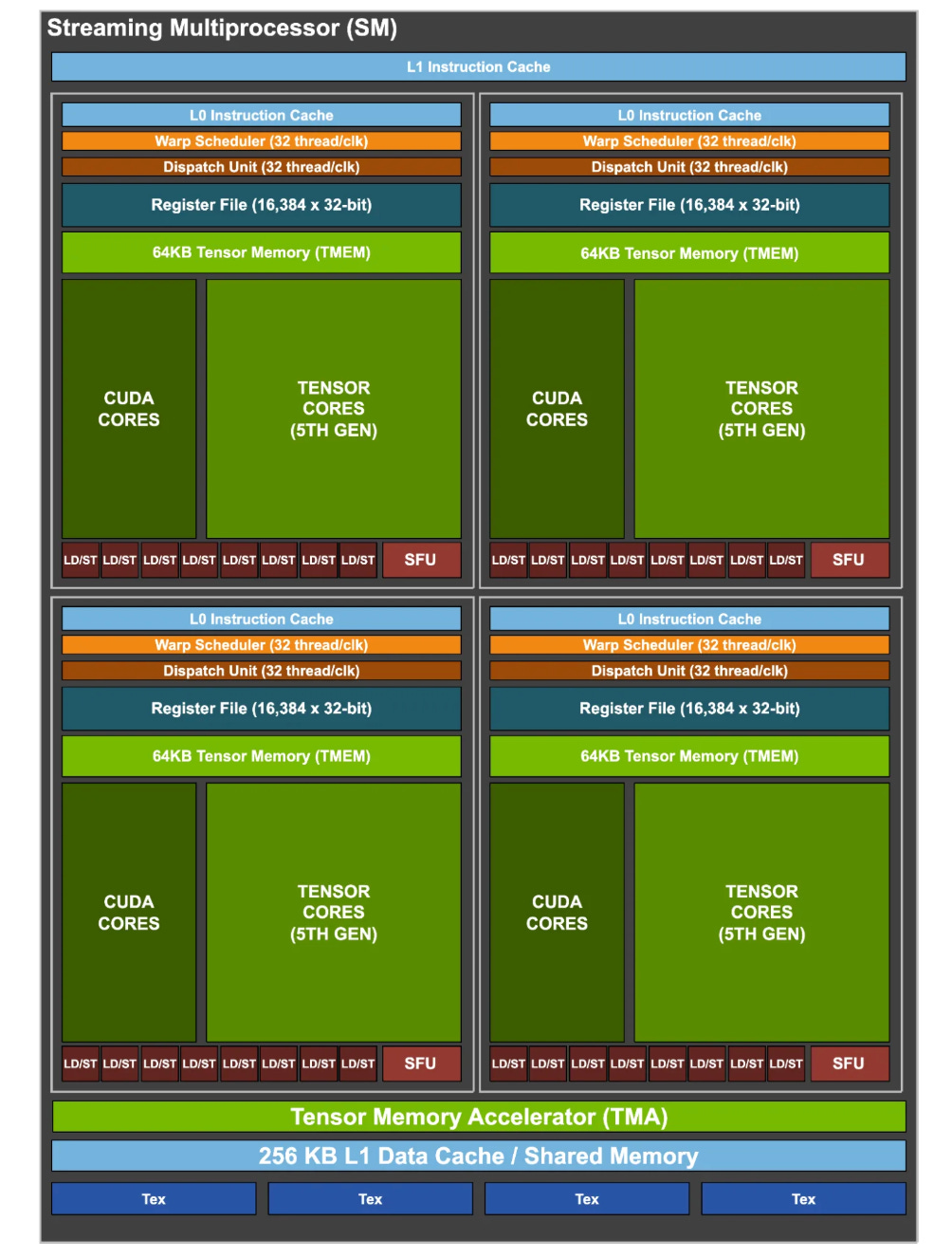
At the GPU clock of 1.98 GHz, on-die SRAM based L1 Cache effectively provides ~37.5 TB/s. This can be derived as follows:
Cache line size, i.e., the width of SRAM = 128 bytes
Clock speed = 1.98 GHz, and the SRAM can be accessed on every clock cycle.
148 Streaming Multiprocessors (SMs)
(128-byte cache line × 1.98 GHz x 148 SMs ≈ ~37.5 TB/s.)
In addition to the existing cache hierarchy, Blackwell’s fifth-generation Tensor Core introduces TMEM, a dedicated 256 KB SRAM per SM designed specifically to serve tensor core operations. Microbenchmarking results indicate that it “provides 16 TB/s read bandwidth and 8 TB/s write bandwidth per SM, and this bandwidth operates additively with L1/SMEM bandwidth rather than competing for the same resources.“ [source]. The introduction of TMEM highlights the performance potential unlocked by highly specialized, on-chip SRAM structures tightly coupled to compute.
Looking beyond GPUs to SRAM-based accelerators, the Groq LPU delivers approximately 80 TB/s of on-chip memory bandwidth, while d-Matrix’s Corsair PCIe card is specified to provide up to 150 TB/s of memory bandwidth.
2. SRAM bandwidth scales alongside compute; HBM is pin limited
Since DRAM chips are external to a logic chip, their performance is fundamentally limited by the interface width, or more specifically by how many I/O pins are practically feasible between memory and xPU. Data rates per pin cannot be pushed faster without degrading signal integrity of the data stream over the copper interconnects that link the memory chip to the xPU.
For example, HBM3e uses a 1,024-bit data bus between the compute die and each memory stack, with each lane operating at up to 9.6 Gbps, yielding about 1.2 TB/s per stack. Increasing bandwidth requires either higher signaling speeds or a wider bus, and the bus width has remained at 1024 bits across four generations — HBM2, HBM2e, HBM3, and HBM3e. Only with HBM4 do we finally see a doubling of the interface width to 2,048 bits as microbump pitches have gotten significantly tighter. Future increases in interface width might only come from switching to hybrid bonding, rather than the thermo-compression bonding that is used today.
SRAM follows a different scaling model from DRAM, because it is integrated directly on the logic die, its bandwidth is not constrained by external pins or fixed memory interfaces. Instead, SRAM bandwidth is largely a function of how many instances are present in the architecture and how closely that SRAM is coupled to compute. As new XPU generations add more compute units, designers can add more distributed SRAM near those units, increasing aggregate on-die bandwidth without relying on faster signaling or wider off-chip buses.
Here is an example: An XPU using 8 stacks of HBM memory has a ~8 TB/s bandwidth that must be shared between all compute units. When SRAM is attached to each compute unit with a 90 TB/s interface bandwidth, the total memory bandwidth increases with the number of compute units - each with their own attached SRAM. So 100 cores would have 900 TB/s memory bandwidth.
In GPUs, this scaling shows up in how cache structures are replicated alongside compute. The Streaming Multiprocessor (SM) is the fundamental execution unit in NVIDIA GPUs, and each SM has its own L1 cache implemented in SRAM. As NVIDIA moved from A100 to H100 to B200, the SM count increased from 108 to 132 to 148. Because each SM has its own L1 cache, increasing the number of SMs also increases the number of SRAM access points that can operate in parallel. This raises total on-die memory bandwidth available to the GPU.
Bandwidth can also be increased by widening SRAM datapaths, for example, by increasing cache line width or the number of banks, further boosting how much data can be delivered per cycle. Taken together, these factors mean SRAM bandwidth can be architected to scale with compute far more closely than DRAM, whose bandwidth is limited by off-die interfaces and fixed pin counts.
3. DRAM theoretical bandwidth ≠ real bandwidth.
In practice, DRAM never delivers its full advertised bandwidth. A portion of that bandwidth is lost to structural inefficiencies inherent to how DRAM works, including:
periodic refresh cycles
bank conflicts
row activation and precharge delays
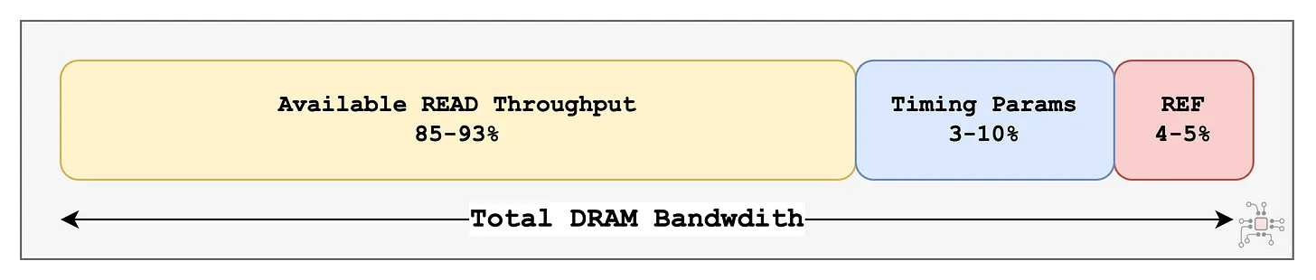
Take refresh as an example. DRAM cells are capacitor-based and leak charge over time, so they must be refreshed periodically to preserve data. For HBM3e, refresh occurs every 3,900 ns (tREFI), during which the memory is unavailable for 350 ns (tRFC). This alone accounts for nearly 8% of bandwidth loss, even before considering any access patterns or contention.
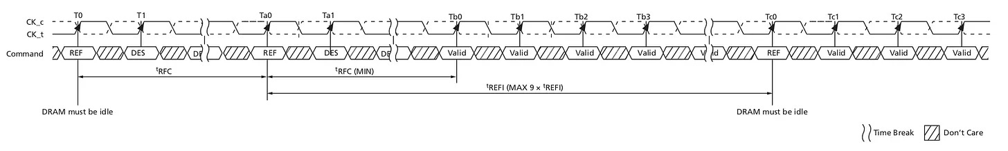
Another major factor is row locality, often described in terms of page hits and page misses. DRAM is organized into rows (or pages). When a row is activated, its contents are loaded into sense amplifiers, allowing subsequent accesses to that row to proceed quickly. If multiple accesses hit the same row, the activation cost is amortized. But when accesses jump between rows, the current row must be closed and a new one activated, an expensive sequence that significantly reduces effective bandwidth. The figure below illustrates the timing difference between a page hit and a page miss.
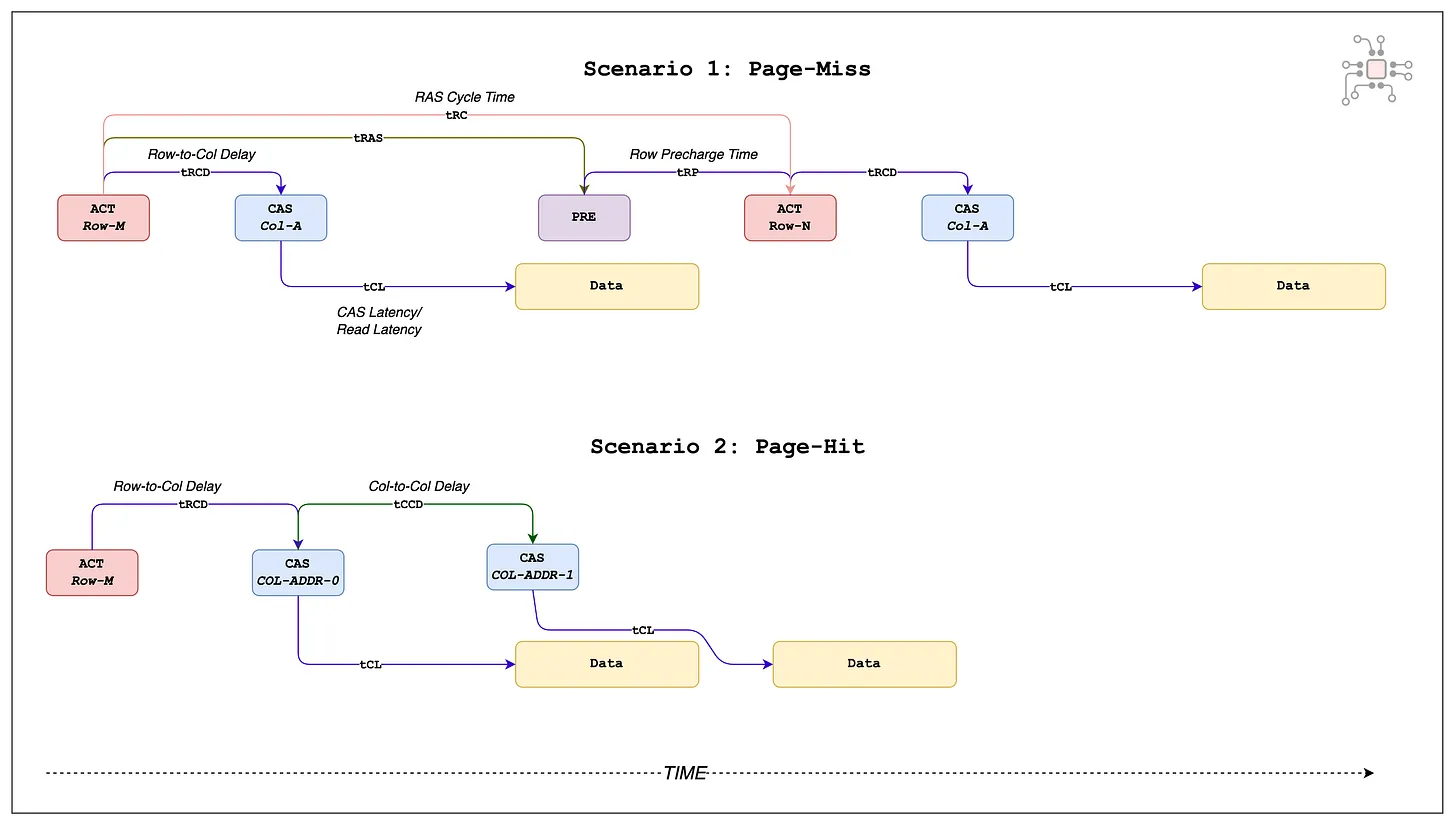
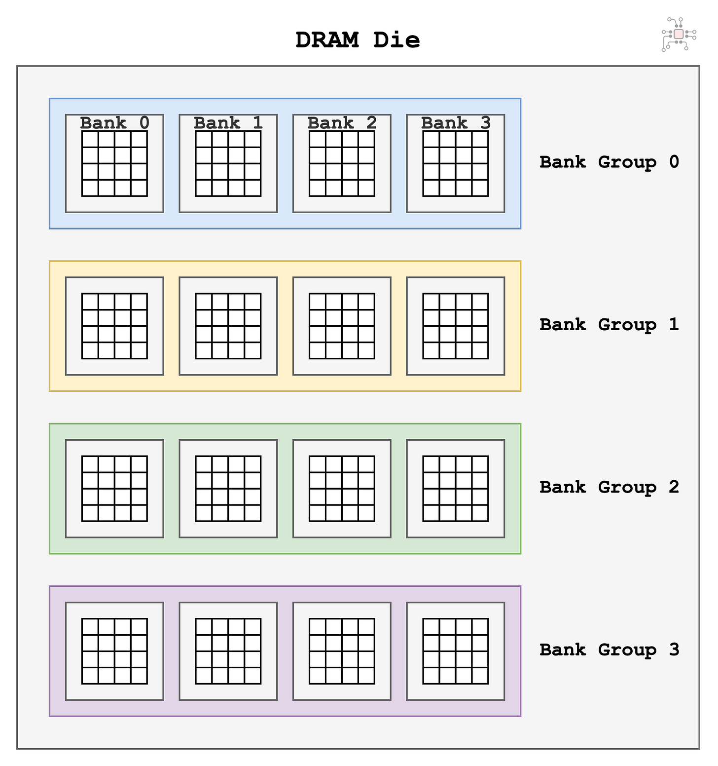
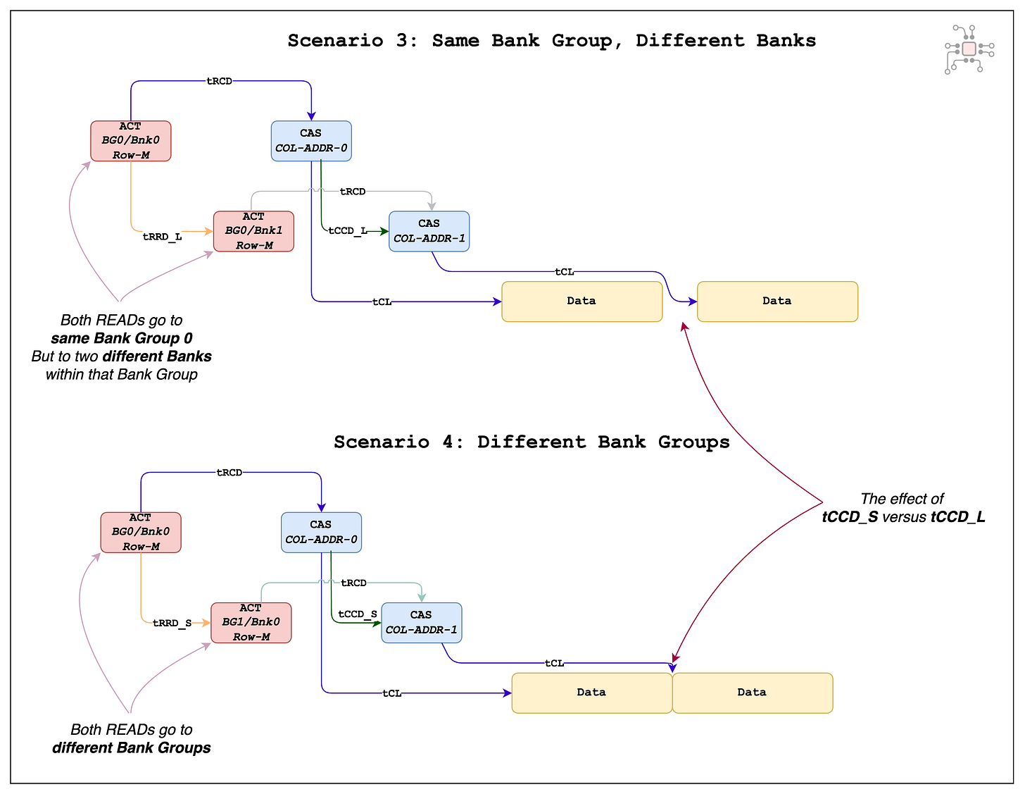
Then there are bank conflicts. DRAM cells are organized into banks and bank groups, and to achieve highest bandwidth, successive memory accesses should target different bank groups.
If accesses hit different banks within the same bank group, an additional delay is introduced. This behavior is captured by the timing parameters tCCD_S (short column-to-column delay) and tCCD_L (long column-to-column delay), as illustrated in the figure below.
These are three examples of why DRAM’s effective throughput can fall well below its theoretical peak. If you need additional details, read this earlier post on Chiplog.

SRAM, by contrast, has none of these structural inefficiencies. There is no refresh, no row activation, and no page-hit or page-miss behavior. If the core can issue a memory request every cycle, SRAM can serve it every cycle. In other words, SRAM’s usable bandwidth is effectively equal to its theoretical bandwidth.
Cost Comparisons: SRAM vs HBM
The whole picture would not be complete if we did not compare the cost per GB of SRAM and HBM. There is an impression from some folks that SRAM has suddenly become attractive given steep rises in DRAM and HBM pricing due to high demand and extreme shortage. Next, we will put together some numbers to show how SRAM cost compares to HBM even amid memory market shortages.
 |
|