
How d-Matrix's In-Memory Compute Tackles AI Inference Economics
A deep look into the architecture from chip construction to rack-scale deployments, performance metrics, and end applications.

Each week, I help investors and professionals stay up-to-date on the semiconductor industry. If you’re new, start here. See here for all the benefits of upgrading your subscription tier!
Paid subscribers will get have access to a video discussion of this essay, key highlights, and a google drive link to this article to parse with LLMs.
Disclaimer: This article is entirely my own opinion. I have not been paid by d-Matrix, nor do I have any access to internal documents. All information is publicly available (references cited). I do not hold any investment position in d-Matrix, and this is not investment advice. Do your own research. This article does not reflect the views of any past, present, or future employers, nor does it directly or indirectly imply any competitors are better or worse. This is my attempt at trying to understand how core technology works and where its advantages lie. I do not endorse any products.
Disclosure: I requested that d-Matrix review the article to ensure that I do not misunderstand/misrepresent their technology. I’m grateful to them for pointing out errors in my conceptual understanding. All editorial decisions are entirely mine.
Recently d-Matrix, a Bay Area AI inference chip startup, announced its Series C funding of $275M which brings its total funding up to $450M.
d-Matrix claims to have the “world’s highest performing, most efficient data center inference platform for hyperscale, enterprise, and sovereign customers,” and a “full-stack inference platform that combines breakthrough compute-memory integration, high-speed networking, and inference-optimized software to deliver 10× faster performance, 3× lower cost, and 3–5× better energy efficiency than GPU-based systems.”
Their main compute engine is called Corsair, and is based on a different approach to inference called in-memory compute. In this post, we will look at this technology in detail, how it provides all those benefits, and where it is useful.
For free subscribers:
Analog in-memory computing
d-Matrix’s digital in-memory compute solution
Four chiplets and LPDDR5
Scaling up to rack-level solutions
References
For paid subscribers:
A real-world use-case for d-Matrix DIMC hardware
Designing Hardware for Latency, Throughput, and TCO
The PCIe Advantage
Possible Uses of Small Inference Models running d-Matrix Hardware
Analog In-memory Compute (AIMC)
The process of AI training and inference involves a lot of matrix multiplications, followed by additions, which come from vector multiplications. If you need a deeper understanding of what those operations are in the context of transformers, check out my earlier primer.

These operations are called multiply-accumulate (MAC) operations. It turns out that GPUs are really good at doing this with specialized arithmetic units that run massively in parallel, which is why we see a huge demand for GPUs in AI applications. A lot of effort has gone into making this operation as efficient as possible. Interestingly, nature gives us a way to do this in the analog world that is simple and with much lower power consumption.
The analog multiply operation stems from Ohm’s law expressed in the current-voltage relation form: I=GV, where I is the current, G is the inverse of resistance called conductance, and V is the voltage. The analog accumulate operation comes from Kirchhoff’s current law: current entering a node is the sum of all currents exiting it, or, Itotal = I1+I2+ … +IN. This is a simple MAC operation that can be done entirely with passive elements and is called current-based analog in-memory compute.
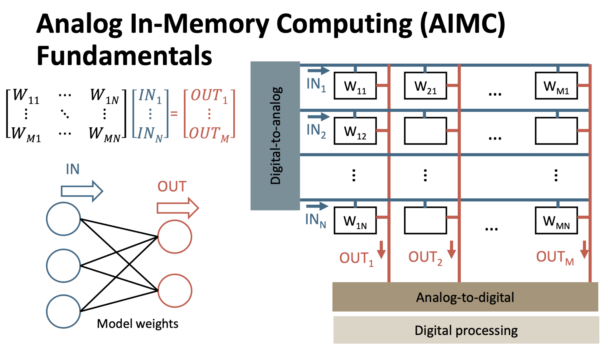
The matrix W can be implemented in a variety of ways - with resistors, flash memory, SRAM, memristors, and even simple transistors. If their value is set appropriately, they are basically “weights” that can be used in AI inference. In such an analog MAC operation, the entire matrix can be computed nearly instantaneously while consuming minimal power because there are no switching transistors. The main reason this has not become the de-facto computing standard is because conductance (G) varies in the analog world. Noise, temperature, and variability all make current-based AIMC challenging.
There is another variation called charge-based AIMC. The idea is to use capacitors as weights instead of resistors, and rely on the charge-voltage relationship Q=CV for multiplication, and the law of charge conservation for accumulation: Qtotal = Q1+Q2+Q3+ … +QN. This approach too, presents its own challenges related to process stability, charge leakage, and noise.
There are a whole lot of other approaches in literature involving phase-change memory, spin-transfer torque RAM, and a host of others that use the analog properties of these components to perform computing. All these methods are still in research or early startup phases.
d-Matrix initially pursued a charge-based analog approach. The result was their first proof-of-concept chip: Nighthawk. However, they quickly abandoned it because it was challenging to fit analog-to-digital converters (ADCs) into each bitline of the memory array - a problem that was more trouble than it was worth, or at least that’s what d-Matrix decided at the time. Companies like encharge.ai and aistorm.ai are still pursuing analog computing for AI, and research conferences are rife with new approaches; so it’s not entirely out of the running just yet.
d-Matrix’s Digital In-Memory Compute (DIMC)
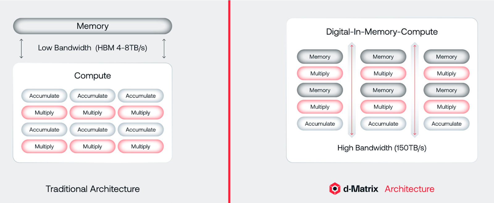
An alternative is to perform MAC computations in the digital domain. Going digital alleviates a lot of the “variability” problems that plagues analog approaches, while being able to scale with newer technologies. There are opportunities to perform calculations in the memory controller or in the base die of HBM, which may be useful for some basic operations like data reshaping or pre-processing, and could be considered in-memory compute. But this is not really what we will talk about because base dies do not provide sufficiently high-end performance for AI inference solely for the reason that these logic chips often used with memory are not inherently compute-focused (in HBM4, base dies are built with advanced logic nodes and there is more juice for compute).
d-Matrix’s digital in-memory compute approach is still based on a “Von Neumann” architecture where data is accessed from memory and processed in logic. However, instead of keeping memory external to the processing chip as DDR or HBM, SRAM cells are woven into the compute function, as shown below.
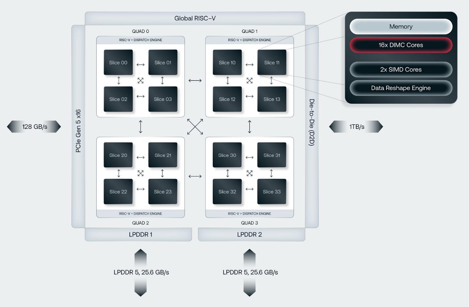
This might look to some like computing from L1-L3 SRAM cache which has been predominant in general computing architectures for decades, but there is a nuance to d-Matrix’s approach here. Instead of allocating a portion of the chip to SRAM and a portion to compute, d-Matrix has finely-tuned digital in-memory compute (DIMC) cores consisting of MAC functions and SRAM that are designed to handle very specific numeric array sizes - 64 × 64 to be exact. For example, a single chiplet has 256 DIMC cores and 256 MB of SRAM.
The block diagram below shows more architectural details. A single chiplet is split up into four quads, each having four slices. The slices and quads all talk to each other in an “all-to-all” interconnect system so that all 256 DIMC cores act as a single logical entity. In addition, there are three interconnect interfaces:
Die-to-die: Allows weaving together more DIMC cores by adding chiplets.
LPDDR5: Allows for memory expansion beyond SRAM, to external DDR.
PCIe Gen5 x16: Allows connectivity to the external world, in compute racks.
There is a global RISC-V engine that orchestrates all the functions in the chiplet, and external interfaces including loading model weights into SRAM.
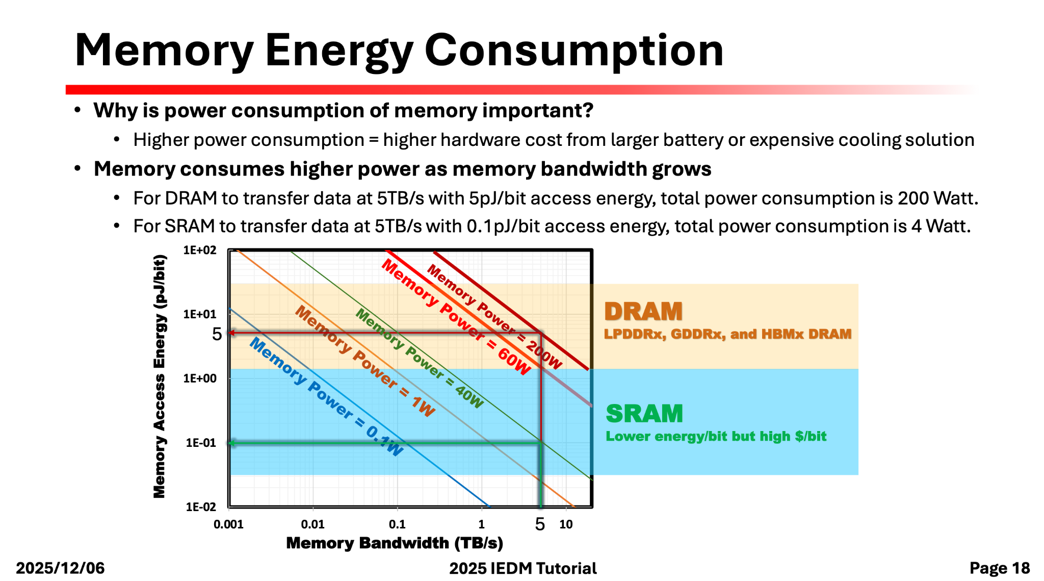
Accessing data from SRAM means that d-Matrix chips provide a memory bandwidth up to 150 TB/s; much faster than the best-HBM based implementations which only achieve about 2 TB/s per chip, or up to 8 TB/s if four HBM die are packaged with the GPU on the interposer. This kind of memory bandwidth drastically increases the tokens-per-second generated, and has unique applications where latency is paramount. The penalty paid for this memory bandwidth is capacity since SRAM is inherently low density.
Additionally, the energy cost of pulling data from HBM of about 3 pJ/bit is a disadvantage in traditional architectures. Having most computations performed in SRAM dramatically reduces the energy required to shuffle bits in and out of the chip. d-Matrix claims they have an energy cost of 0.3 pJ/bit; 10 times lower than a HBM based approach.
Four Chiplets and LPDDR5
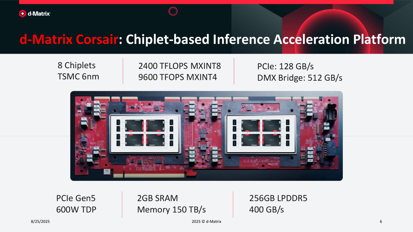
The limited 256 MB SRAM on the chip is significantly crippling when it comes to loading model weights. A 120 billion parameter GPT-OSS model requires about 65 GB of memory to load all the model weights; even the 20 billion parameter version uses 14 GB. d-Matrix’s approach is to use multiple chiplets to expand the compute and memory capacity of their DIMC inference chips. This architecture is shown below and is a key component of their Corsair compute platform.
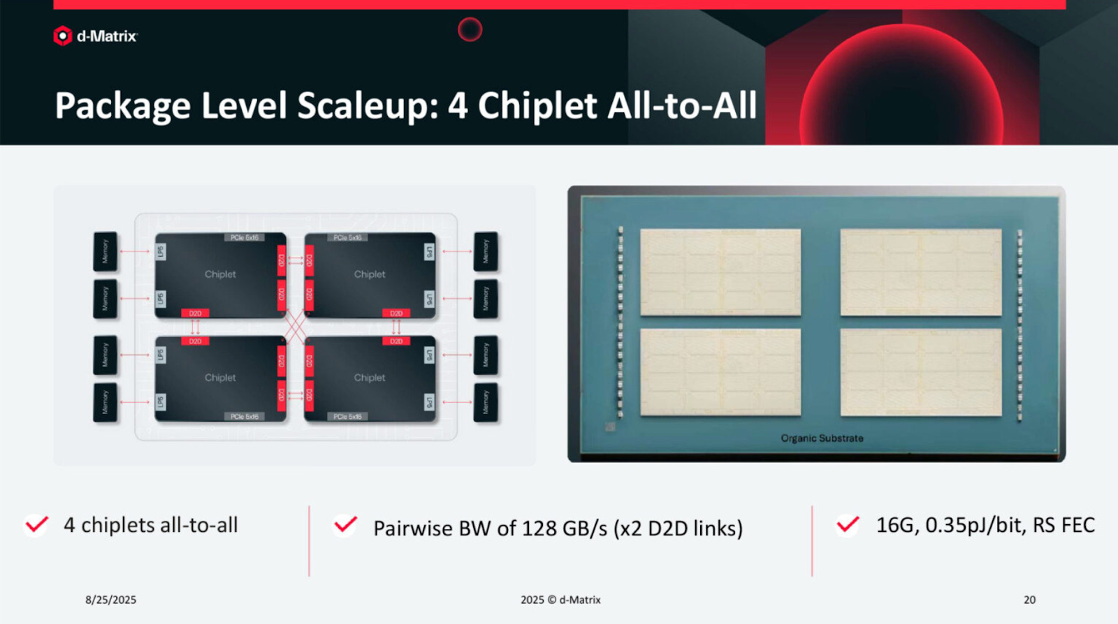
There are four chiplets hooked up together on an organic substrate package, which means that the total SRAM capacity is increased to 256 MB × 4 = 1 GB. The die-to-die interconnect IP called “DMX Link” is a custom built in-house solution that achieves a total bandwidth of 1 TB/s. Each chiplet is still pretty big - in the range of 400 sq. mm, which is about half the size of the reticle.
There are two other aspects that reduce the cost of this system.
The chiplets are connected together on organic substrate which is far less complex and lower cost compared to CoWoS interposers used to interface HBM to compute die.
The extended LPDDR memory is packaged on the board level. LPDDR is nowhere near the cost of HBM and packaging it on the board is an inexpensive approach.
Let’s talk about LPDDR memory. 1 GB of SRAM from four interconnected chiplets is still not sufficient to hold sizable models. d-Matrix provides off-chip DRAM to hold model weights, but this comes with performance (in this case latency) penalties. But, whether you choose to use more Corsair chips for an all-SRAM approach to inference, or utilize fewer Corsair chips with a largely LPDDR approach depends on the workload needs. Through their Aviator software platform, the Corsair can be operated in Performance or Capacity mode accordingly.
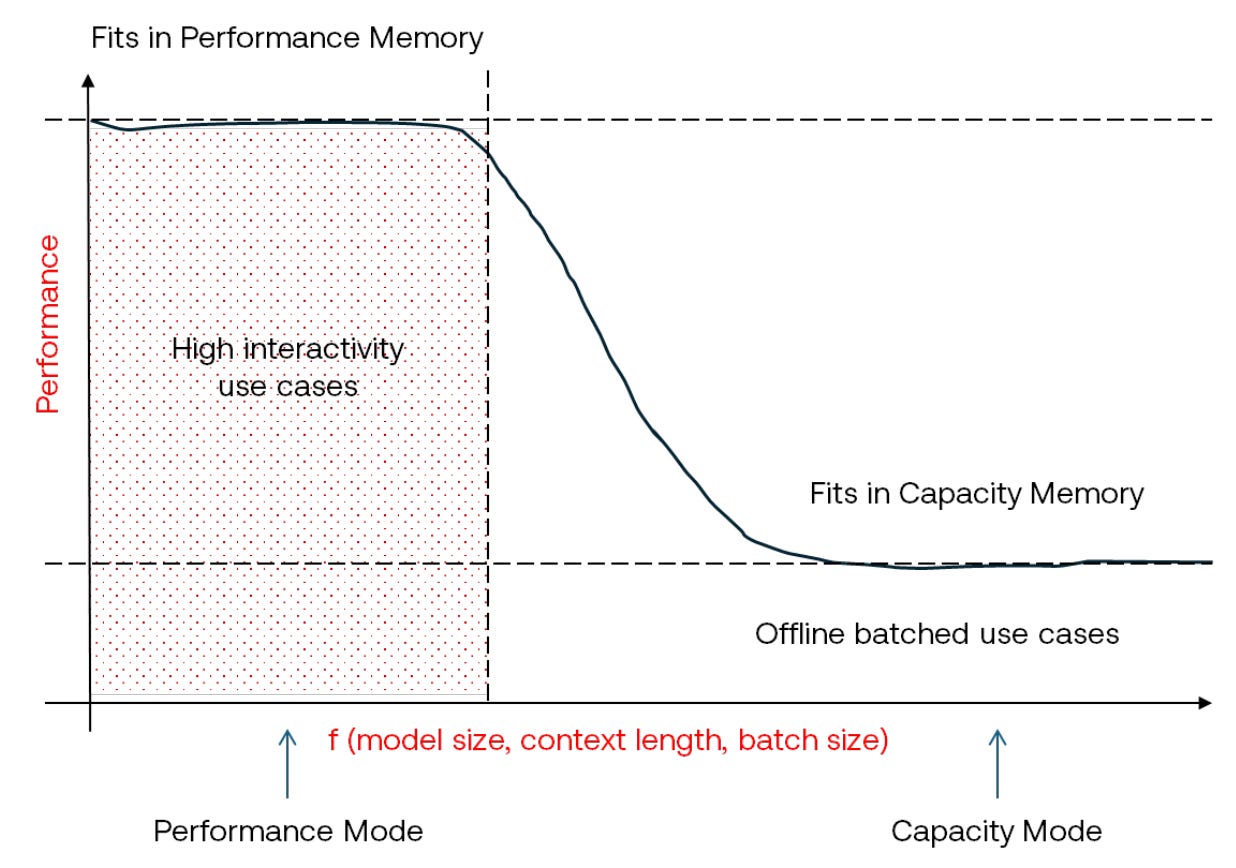
At first glance, this looks to some experts like a glaring shortcoming of d-Matrix’s approach. Since SRAM densities have largely stopped scaling, why use this at all, especially knowing that you simply cannot get the kind of memory density that HBM offers? The subtlety here is that the Corsair platform allows the inference system to be built out according to the workloads it is designed for. Fine-tuned AI accelerator architectures are becoming increasingly important over “once-size-fits-all” racks, and is a key reason why the d-Matrix approach is attractive. We will revisit this in greater depth beyond the paywall.
In my discussions with d-Matrix, they pointed out another useful feature of having performance and capacity modes: disaggregated compute. Increasingly, inference architectures now separate prefill and decoding steps into distinct hardware, as we have seen with Nvidia CPX that uses DDR instead of HBM. The prefill step is compute bound and does not rely on memory bandwidth, for which Corsair can be operated in capacity mode. For the decode step, the extremely high memory bandwidth available in performance mode is well suited.
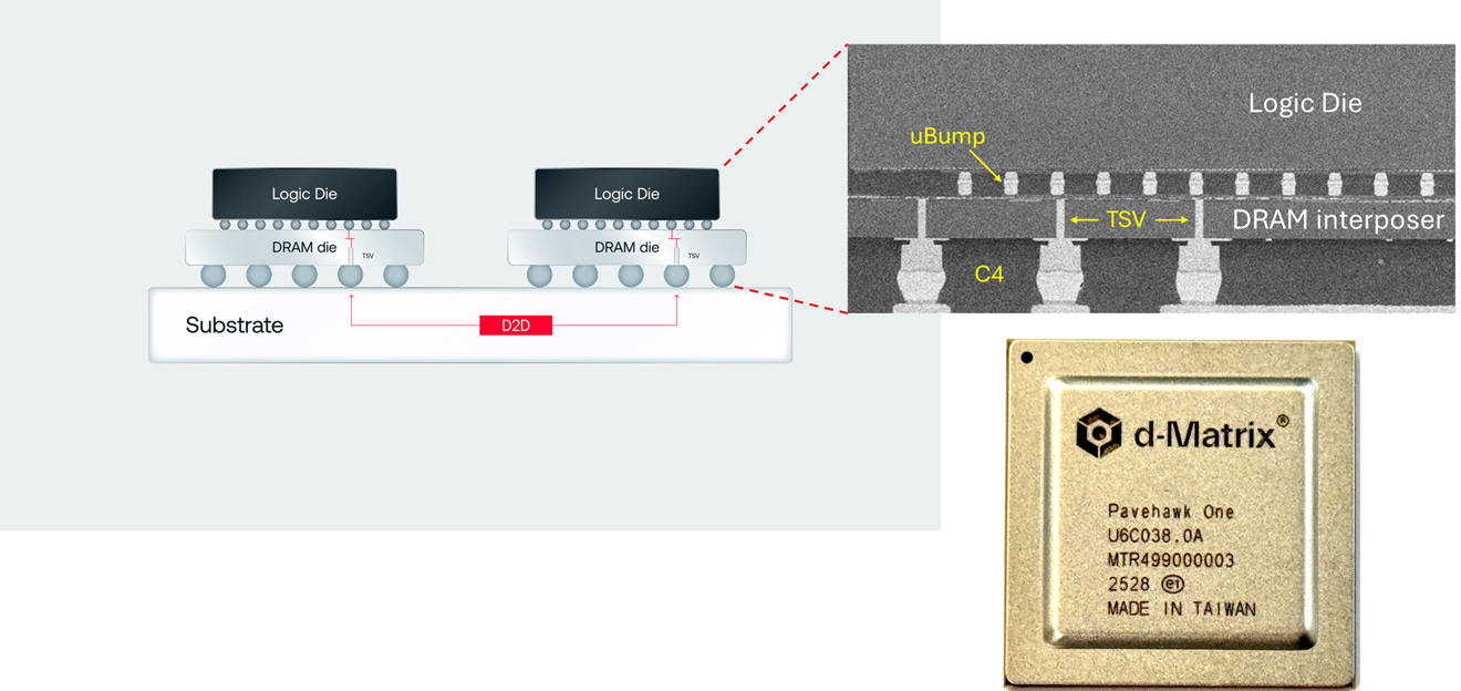
d-Matrix’s next generation testchip, PaveHawk, integrates the DRAM under the logic die. It could even be a multi-stacked DRAM die that is reminiscent of HBM, that will provide a much greater memory bandwidth and improved performance when running larger models or big context windows. If a ~400mm2 compute chiplet is stacked over an equally sized DRAM chip, there will be an enormous number of parallel lanes using through silicon vias (TSVs) over which memory can be accessed with high bandwidth while maintaining high capacity. The question remains if such large memory chips can be reliably packaged with compute die in the presence of thermal constraints.
d-Matrix calls this 3D-in-memory compute (3DIMC), and the learnings from the PaveHawk One testchip will be incorporated into their next generation architecture called Raptor.
Scale-Up to Rack-Level Solutions
So far, we have discussed up to the chiplet on a substrate. d-Matrix’s actual solution is a PCIe card built on a 24-layer board with two such substrates - with 8 compute chiplets, a total of 2 GB SRAM, and a configurable amount of external LPDDR memory that is on the back of the card. The two substrates in a single card are connected via PCIe5 x16, for a total power dissipation of 600W. This allows all 8 chiplets to operate coherently.
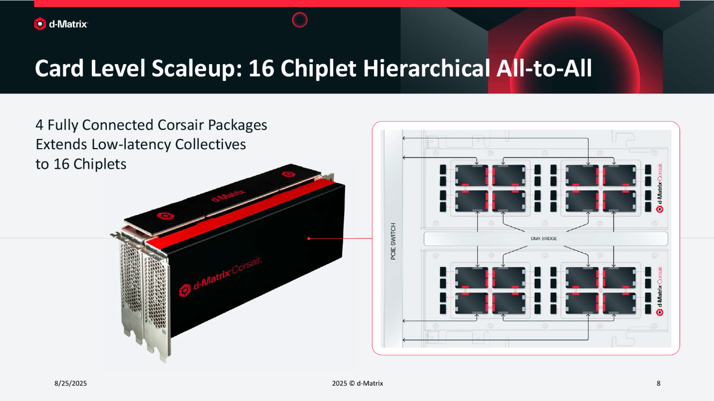
Two such PCIe cards can then be merged to act as one using a special DMX Bridge card that hooks up to the open PCIe interfaces on each chiplet, on the top of the card, so that a dual-Corsair package has a total of 4 GB SRAM, and 4,096 DIMC cores from 16 chiplets configured in an all-to-all connection.
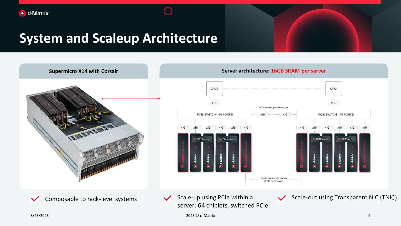
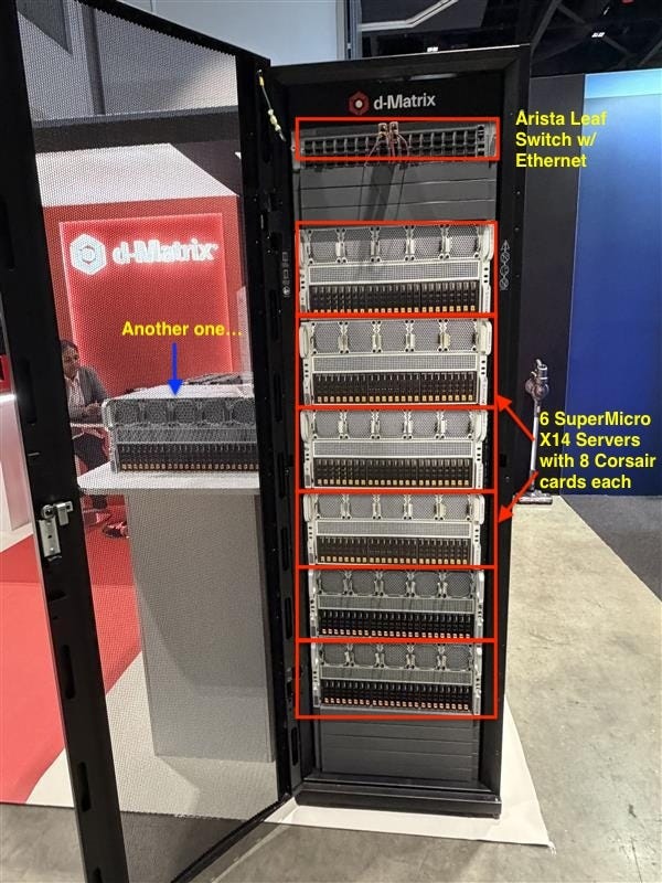
PCIe interfaces imply that these cards can be easily placed into a standard server rack-case like the Supermicro X14 shown below. This brings the total amount of SRAM to 16 GB in one such server. Each server also has d-Matrix’s JetStream PCIe card (other NICs would work too), which is a network interface card that allows accelerator cards to talk to each other through Ethernet, allows scale-out outside the server rack, and also links to the top-of-rack leaf switch.
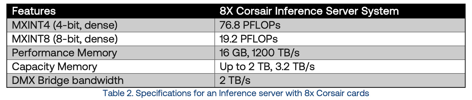
The performance obtained from one such compute server with 8 Corsair cards is published by d-Matrix as shown in the table below. How these numbers translate to inference speeds is nuanced, and will be discussed after the paywall.
Even an 8x Corsair system does not have enough SRAM to house anything except the smallest parameter model - the GPT-OSS 20b comes to mind, or other similar small, but highly specialized models. The system only gets usable for 100 billion parameter-class models when you put about 6-8 of these servers in a single rack as shown below. Now you have about 100 GB of SRAM that can house competitive medium sized models, that you can use to perform inference at blazing speeds.
So far, we have seen how d-Matrix’s DIMC cores scale from a single chiplet, all the way to a rack scale solution. A bit of detail that we did not address is how d-Matrix uses block floating point numerics. It is sufficient to know that this unique number format reduces the memory needs and is well suited to their SRAM-centric inferencing approach.
The references below were used to write the contents of this post. After the paywall, we will explore some potential uses for d-Matrix hardware:
A real-world use-case for d-Matrix DIMC hardware
Designing hardware for latency, throughput, and TCO
The PCIe advantage
Possible uses of small inference models running d-Matrix hardware
References
d-Matrix® Corsair™ Redefines Performance and Efficiency for AI Inference at Scale (Whitepaper)
Serve the Home Post on d-Matrix from Hot Chips 2025
LLM Inference Performance Engineering - Best Practices (Databricks)
Block Format Error Bounds and Optimal Block Size Selection (arxiv)