
High Bandwidth Flash: NAND’s Bid for AI Memory
Can HBF be a new memory tier for AI workloads? Where its limits will show, and what are use-cases for a high capacity memory thats slower than HBM or GDDR.

Welcome to a 🔒 subscriber-only deep-dive edition 🔒 of my weekly newsletter. Each week, I help investors, professionals and students stay up-to-date on complex topics, and navigate the semiconductor industry.
If you’re new, start here. As a paid subscriber, you will get additional in-depth content. We also have student discounts and lower pricing for purchasing power parity (see discounts). See here for all the benefits of upgrading your subscription tier!
Last month, Sandisk teamed up with SK Hynix through a Memorandum of Understanding (MoU) to co-develop a new kind of memory called High Bandwidth Flash (HBF) for AI applications, which uses NAND-based technology most commonly found in SSDs.
High Bandwidth Memory (HBM) is used in GPUs within AI accelerators today, which in particular contains many thin DRAM chips stacked up vertically. Other than the GPU itself, HBM is a central part of AI training and inference. Its high data bandwidth ensures that the GPU readily has the data available for computations.
HBM is an order of magnitude costlier than commonly available DDR memory, but its real downside is capacity. For example, Nvidia’s Blackwell GPU has eight stacks of 24 GB HBM3e chips (each contains 8 DRAM chips of 3 GB capacity stacked vertically) resulting in a total of 192 GB of memory. As model sizes explode, context lengths increase, and AI video generation takes off, there is a need for lot more memory. But DRAM memory density scaling has largely ended.
NAND-based HBF promises an alternative; not just as storage, but as a new memory tier. NAND flash is a denser memory technology that can supposedly provide 8-16 times more memory in the same footprint as HBM. It is, however, not without downsides. HBF is not in production, but first samples from Sandisk are expected in the second half of 2026, with first inferencing results likely in 2027.
In this post, we will discuss what HBF might look like, its primary shortcomings and potential use-cases.
For free subscribers:
Why DRAM and HBM is Suitable for AI Applications
How NAND and High-Bandwidth Flash (HBF) is Different
For paid subscribers:
Hybrid HBM + HBF Architecture: Can HBF replace HBM along the GPU shoreline, or work in tandem with it?
Can HBF be as competitive as HBM2e? It could perhaps be a lower-cost alternative to state-of-the-art systems.
HBF as a GDDR Replacement in Prefill Compute Chips: Rubin CPX for prefill during inferencing shows that lower memory bandwidth performance is sufficient. HBF could have a potential use case.
Brief outlook: Where we are, what needs to be done, and by when.
Read Time: 11 min
Why DRAM and HBM is Suitable for AI Applications
DRAM consists of a transistor and capacitor (called the 1T1C cell) hooked up in a large array on a chip. The charge stored in the capacitor represents the bit value of the cell. Due to the physical construction of the stacked capacitor, the charge eventually leaks away unless it is refreshed within milliseconds - hence the term dynamic RAM, or DRAM. Read this post by Chip Log if you want to learn more about the fundamentals.
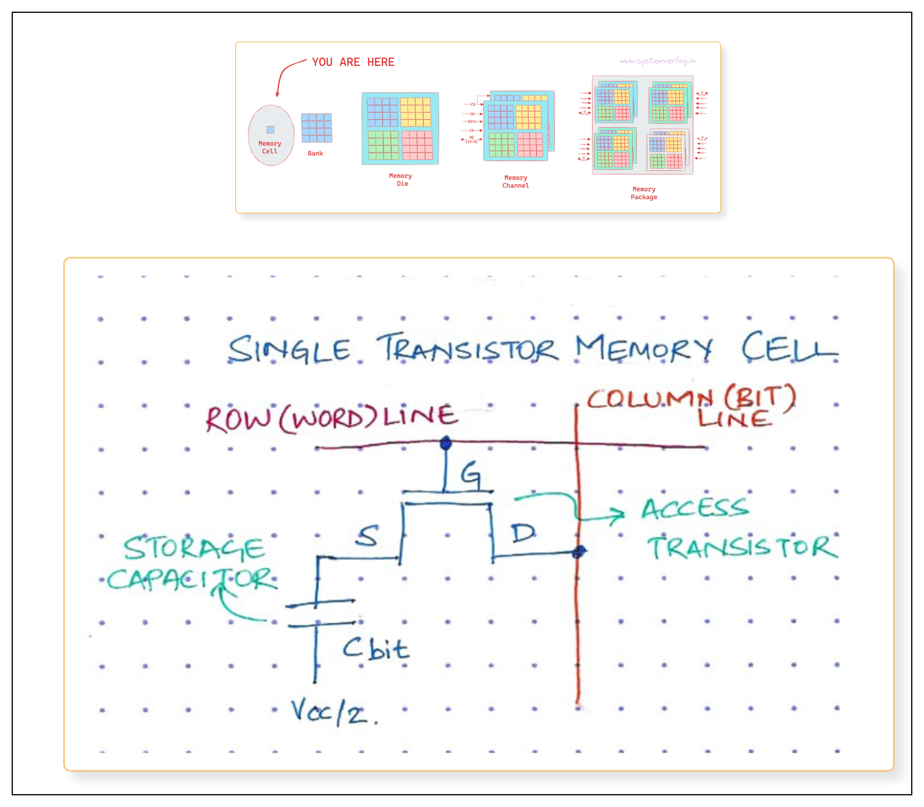
DRAM’s biggest downside is capacity. The main reason that the density of DRAM has stopped increasing is the difficulty in making the 1T1C cell any smaller. However, DRAM has three big advantages that makes it absolutely essential:
Bandwidth: The data rate available is extremely fast. For example, GDDR7 uses DRAM and provides a bandwidth of 32 Gbps per pin.
Latency: DRAM offers nanosecond level latency which is great for AI applications. It is also possible to read just a few bits from DRAM with minimal latency due to individual access to each row and column in the array.
“Infinite” Endurance: It is well suited to reads and writes without any concern of endurance, which is important considering how much data crosses memory in AI workloads.
Thus, stacking DRAM chips to create HBM is the logical way to retain all the benefits of DRAM and simply increase capacity. Stacking is a complex manufacturing process, and yield drops as stack heights get bigger, making HBM very expensive. For a better understanding of HBM, read my earlier post below.

How NAND and High-Bandwidth Flash is Different
The unit cell of NAND flash is a single transistor with a “floating gate” that can trap or release electrons. The presence or absence of an electron changes the threshold voltage of the transistor (the voltage to turn it “on”), which can then be read out. In a sense, the transistor itself stores charge and no special capacitor is needed. These floating gate transistors can be packed tightly together to achieve high memory density. For an excellent history of NAND flash, watch this video by Asianometry.
More than one bit can also be stored in such a transistor which means that each transistor holds more data overall. A Multi-Level Cell (MLC) holds two bits, which can be read out as four different threshold voltage shifts. Triple-level (TLC), Quad-level (QLC) or Penta-level (PLC) cells also exist for higher memory density. These memory cells are then chained together to create NAND logic functionality.

Since there is no cumbersome capacitor present, many layers of NAND cells can be stacked on top of each other by depositing alternating layers of silicon nitride and oxide. SK Hynix recently announced a 321-layer QLC NAND flash for SSD applications, which results in 2 Terabytes of storage in a single chip. When multiple multi-layer NAND chips are stacked on top of each other much like HBM and connected with through-silicon-vias (TSVs) and microbumps, we get HBF.
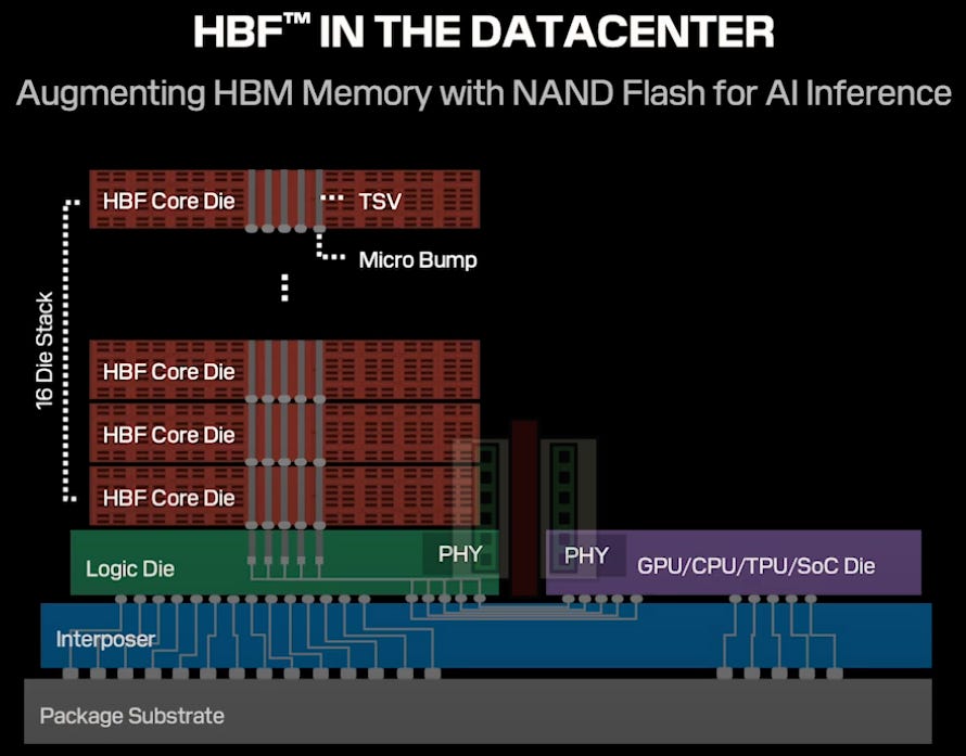
Stacking NAND Memory with TSV
You might ask: if NAND memory is already stacked up to 321 layers, why are we stacking it again using TSV and microbumps?
The answer lies in parallelism. Just like in HBM, we need to access data stored in HBF simultaneously via multiple pins - up to 2,048 of them in the case of HBM4. Even if the data rate at each pin is slow, parallel access increases the total data throughput - like using a large diameter firehose with medium pressure water flowing through it.
For this to work in HBF, the cell array needs to broken up into multiple I/O channels, as shown by SanDisk below.
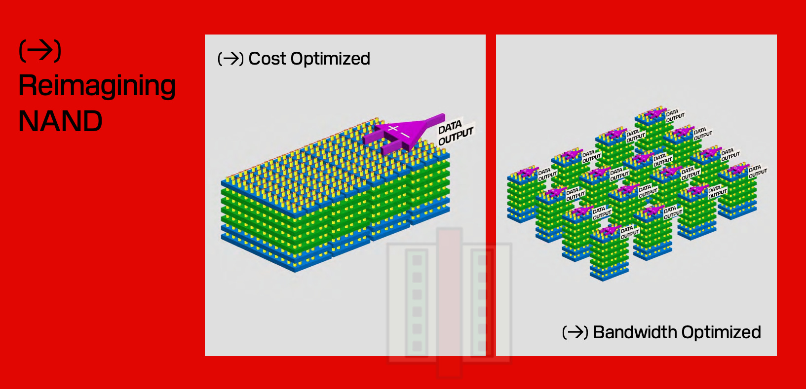
Since NAND provides extraordinary data capacity compared to DRAM, stacks of 12 or 16 chips like in HBM are unnecessary when creating HBF. If each layer is 256 GB, you can get 1 TB storage from only stacking 4 chips - much like the first generation of HBM did with 1 GB DRAM die but produced only 4 GB of memory.
Limitations of NAND
The way NAND memory works imposes serious limitations. The default state of all bits is a ‘1’ and forcing electrons into the gate with an applied voltage sets it to ‘0’. Importantly, a group of cells are chained together to form a page which is usually a few KB in size. Multiple pages form a block (>100 KB). Read and writes occur at the page level, but erasures only happen at the block level by pulling all the electrons out. This mode of operation places limitations in the performance of NAND flash.

Latency: Data access times are in the range of microseconds (1000x longer than DRAM) and depends on the size of data being read from memory. Flash memory is often faster for large blocks of data reads, but gets slower for smaller blocks. Rewriting data requires entire blocks to be erased and rewritten, which slows things down.
Endurance: Electrons are forced in and out of the floating gate using quantum mechanical tunneling through the gate oxide. Repeated write operations cause wear and tear of the oxide material, and eventual failure. DRAM in comparison has “infinite” lifetime.
In spite of these well known limitations, would HBF be useful in AI training and inference?
After the paywall, we discuss:
Hybrid HBM + HBF Architecture: Can HBF replace HBM along the GPU shoreline, or work in tandem with it?
Can HBF be as competitive as HBM2e? It could perhaps be a lower-cost alternative to state-of-the-art systems.
HBF as a GDDR Replacement in Prefill Compute Chips: Rubin CPX for prefill during inferencing shows that lower memory bandwidth performance is sufficient. HBF could have a potential use case.
Brief outlook: Where we are, what needs to be done, and by when.