

This is my first time attending the Hot Chips conference and the overall vibe was a small, tight knit conference with a lot of interactions. No parallel tracks running and continuously having to choose what to attend. The talks from big companies, especially the big three, were pretty detailed; think of it as a collection of heavily technical keynotes.
In this quick note, we will cover presentations from the big three memory players. These are only initial captures from my notes. There is a lot to think about regarding implications and what the proceedings mean for the roadmap, but that takes time.
Contents:
Micron
Samsung
SK Hynix
This is a free post. I hope you enjoy it.
By reading this post, you agree to the terms and conditions. Also see the full ethics statement.
If you’re new, check out the About page. A lot of readers expense the subscription to this newsletter as it helps their professional work. Group subscriptions (3+) are 20% off. If you have any questions, reply to this email and let me know!
Also check out the Semi Doped podcast with and myself, and our daily free newsletter with latest semi news.
If you would like to engage independent research services for your project or need expert calls, check out my boutique consulting practice at SemiExponent.
Micron: We’re so important, we make HBM
This talk was definitely the most unimpressive of the big three, so let’s get it out of the way first. Most of the talk was about the regular culprits like the memory wall, standard roofline curves, and how stacking enables high memory bandwidth. For an audience tuned to AI (aka, most of the lecture hall), this is not news. Only a few things stood out, and we’ll mention those quickly.
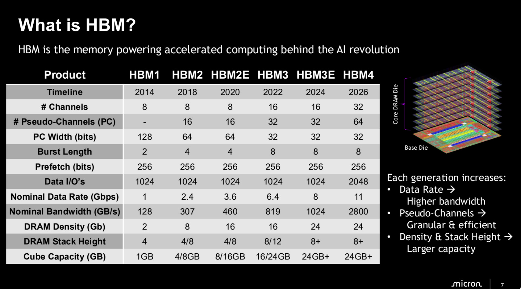
The slide below was one of the more informative comparison slides between the different HBM generations. Most tables like these only cover the overall memory bandwidth, capacity, and stack height. This one compares number of channels, pseudo-channels, burst length, processor controller (PC) width, and bitrate per lane, in addition to the usual numbers. The level of detail is admirable. We will not get into what they all mean here, but the main thing to note is that HBM has a lot more technical metrics that matter to performance than meets the eye on marketing slides.
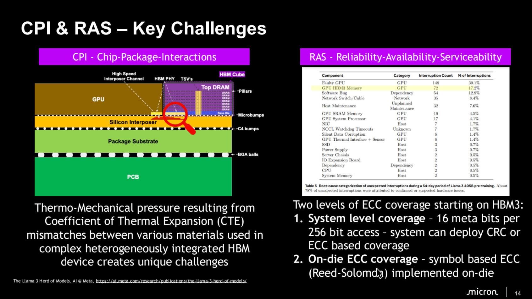
We have discussed why HBM is so hard to manufacture in an earlier post. Of note was the fact that HBM is the 2nd most important root cause of training-run interruptions, apart from the GPU being faulty itself. Software and networking were #3 and #4, respectively. You can read the whole study here.
Notably a few things were absent from Micron’s talk:
Scaling to higher stacks (16-hi/20-hi) and the future roadmap for hybrid bonding.
Any mention of custom base die, and why that is important going forward.
Cooling solutions as HBM lane rates get faster.
At the surface, this might seem like a downside. Given the recent rumors of HBM stack height downgrades, it is questionable if some of these are even required in the future. Except custom base die. That is important, and will continue to exist in logic node implementations — I argue even in lower stack height implementations. Samsung will explain why next.
Samsung: Custom base die on logic nodes because we can
I enjoyed Samsung’s talk so much that I live tweeted the key takeaways from the conference. We’ll briefly expand on these topics here.

Interestingly, they had some charts showing how HBM5 would evolve in terms of spec. Even though nothing is set in stone, it’s fun to see charts up and to the right.
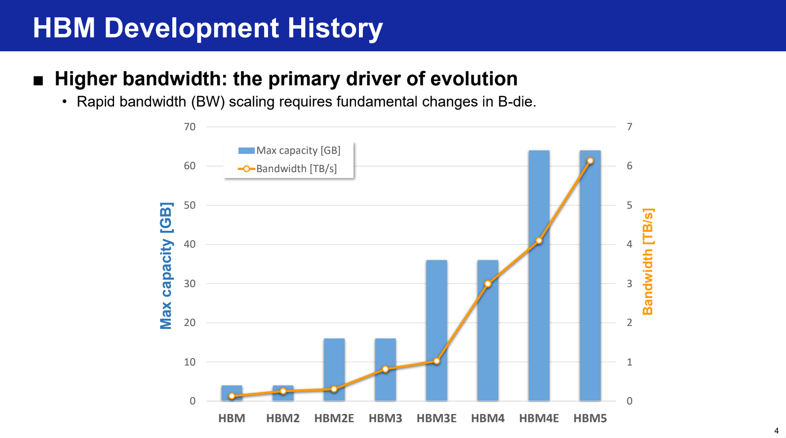
HBM5 with a capacity of 60GB and 6 TB/s bandwidth would be nice. Let’s calculate some numbers here. 6 TB/s with 2,048 lanes would mean 23.5 Gbps per pin. We are currently at 16 Gbps state-of-the-art, and that is a significant step up that is likely possible with an advanced logic node. For 60 GB capacity with 3 GB per die, that would put the stack height at 20 high.
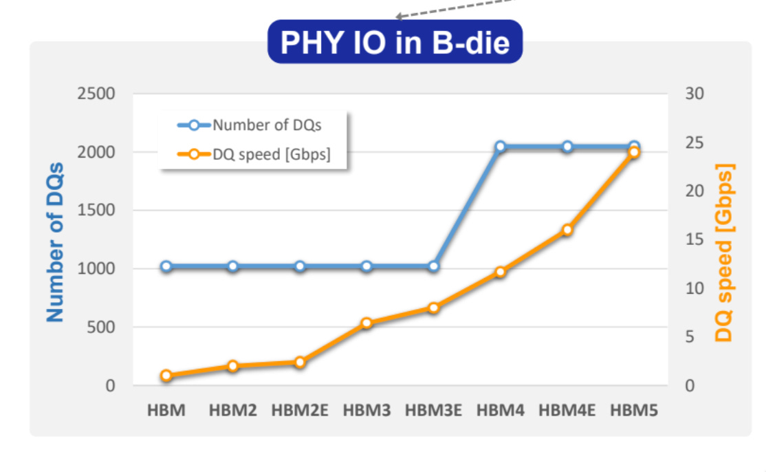
In a separate slide, Samsung confirms that HBM4E is running at 16 Gbps per pin. HBM5 calculations we did above are also validated in the chart below.
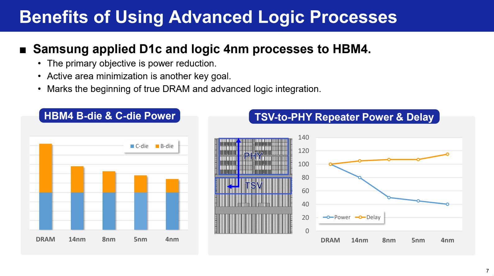
Samsung’s clear advantage is that they have a logic node in-house unlike Micron and SK Hynix who need to partner with somebody to get it. They were sure to play up their advantages here by explaining how custom base die is important going forward. Samsung is using 1c node for memory and 4nm node for logic. It results in a significant power reduction in the base die. The slide below is a silent dig at Micron who used DRAM nodes for logic die in HBM4.
What was even better was how Samsung broke up the roadmap into three clear phases. We’ll cover each one.
Phase 1: The Low Hanging Fruit
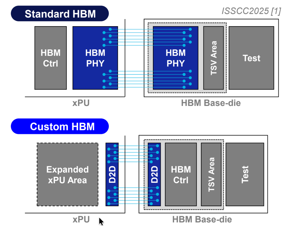
When there is a logic node in the base die, the physical footprint of the HBM PHY block reduces in area and also becomes more energy efficient. This means that the block that works on die-to-die connects between HBM and XPU gets smaller. This have two positives:
Increases the area in XPU for more compute
Increases available area in HBM base die for more advanced functions.
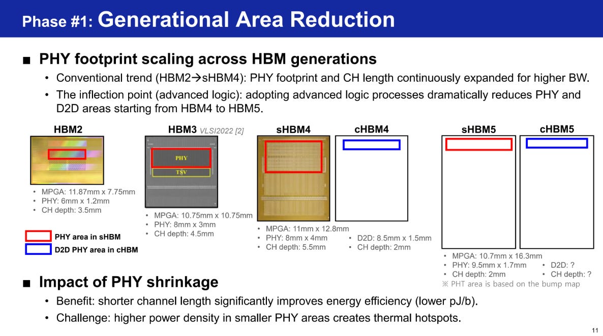
The downside of the shrinking size is more thermal density in these regions. It was interesting that they provided actual sizes of their PHY blocks in various HBM generations.
Samsung also mentioned that they were not inclined to use UCIe for their D2D link because of larger size and poorer energy per bit. They said that their custom PHY implementation was better in performance. When moving to HBM5, they showed the concept of an integrated Heat Path Block (HPB) to cool the D2D PHY region.
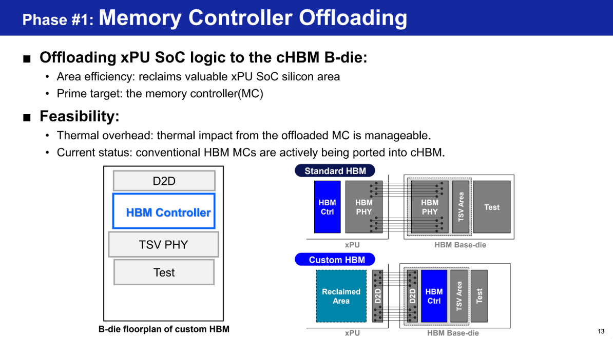
The next big advantage is memory controller offloading which can be moved from the XPU to the custom base die. This reclaims area in the XPU die which can then be used to drive up flops.
The new benefit of having a logic node in the base die is that you can have SRAM. If a particular cell in the DRAM stack is broken, the information in that cell can instead be stored in SRAM and the memory controller will look up SRAM for those cells instead of failed DRAM cells. Think of SRAM as a spare notebook which acts as a scratchpad to hold data that could otherwise not be held in defective DRAM cells.
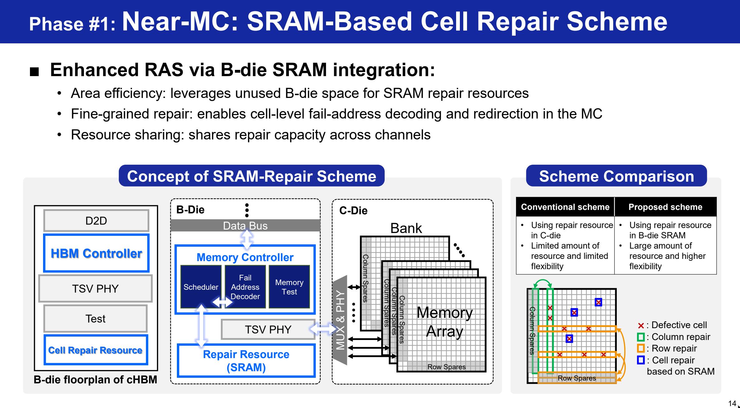
Phase 2: RAS, Test, Extension, Processing
The use of a logic node for base die means that silicon area used for a lot of these functions is smaller if the transistors are smaller. The extra space available is useful for a few things like Repairability-Availability-Servicability (RAS), testing, and collecting telemetry data about the health/status of the HBM memory stack. HBM telemetry data will be very useful given that it is the #2 thing to kill a training run.
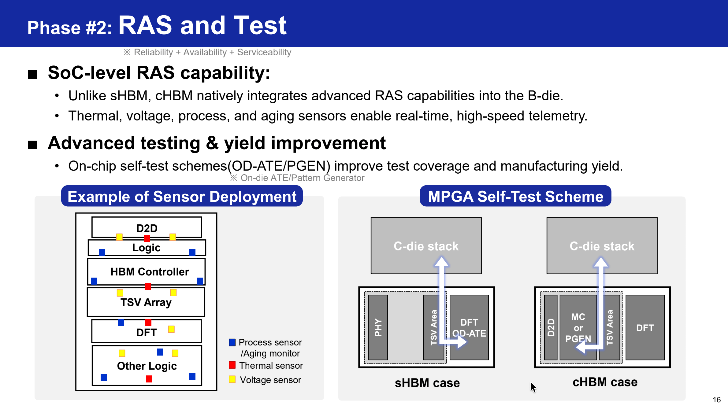
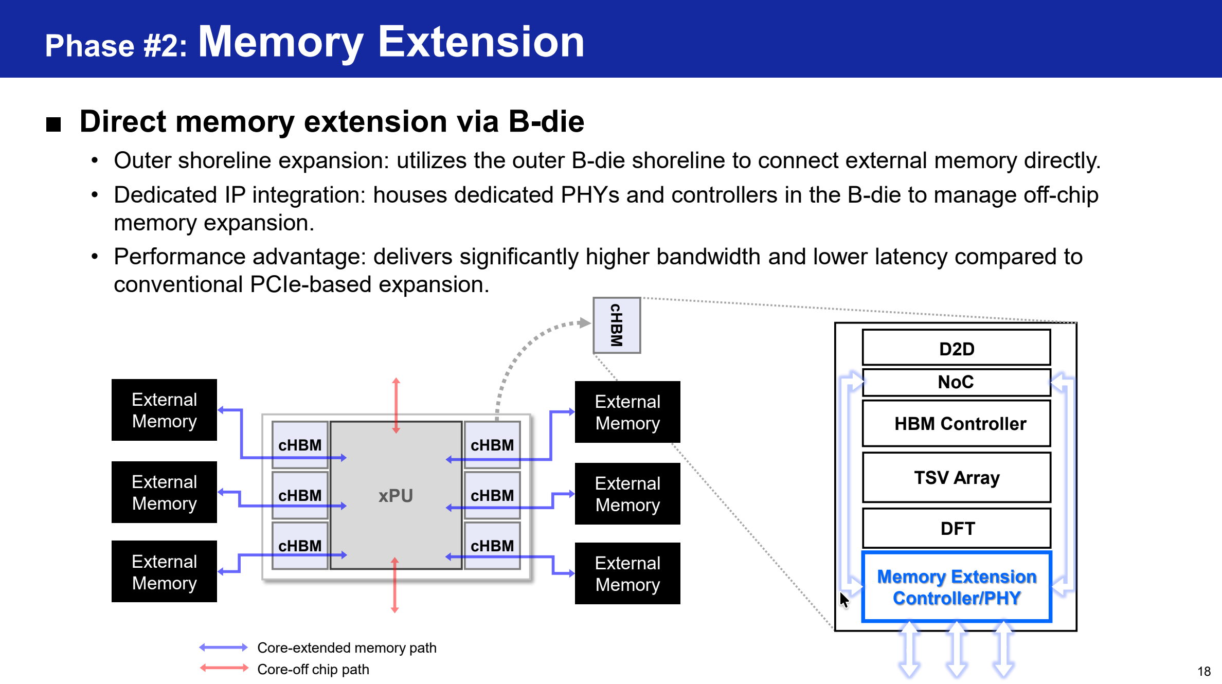
If there is even more silicon area left over, then one can build another memory extension controller to connect another HBM stack behind the first one or put in a DRAM chip to extend memory.
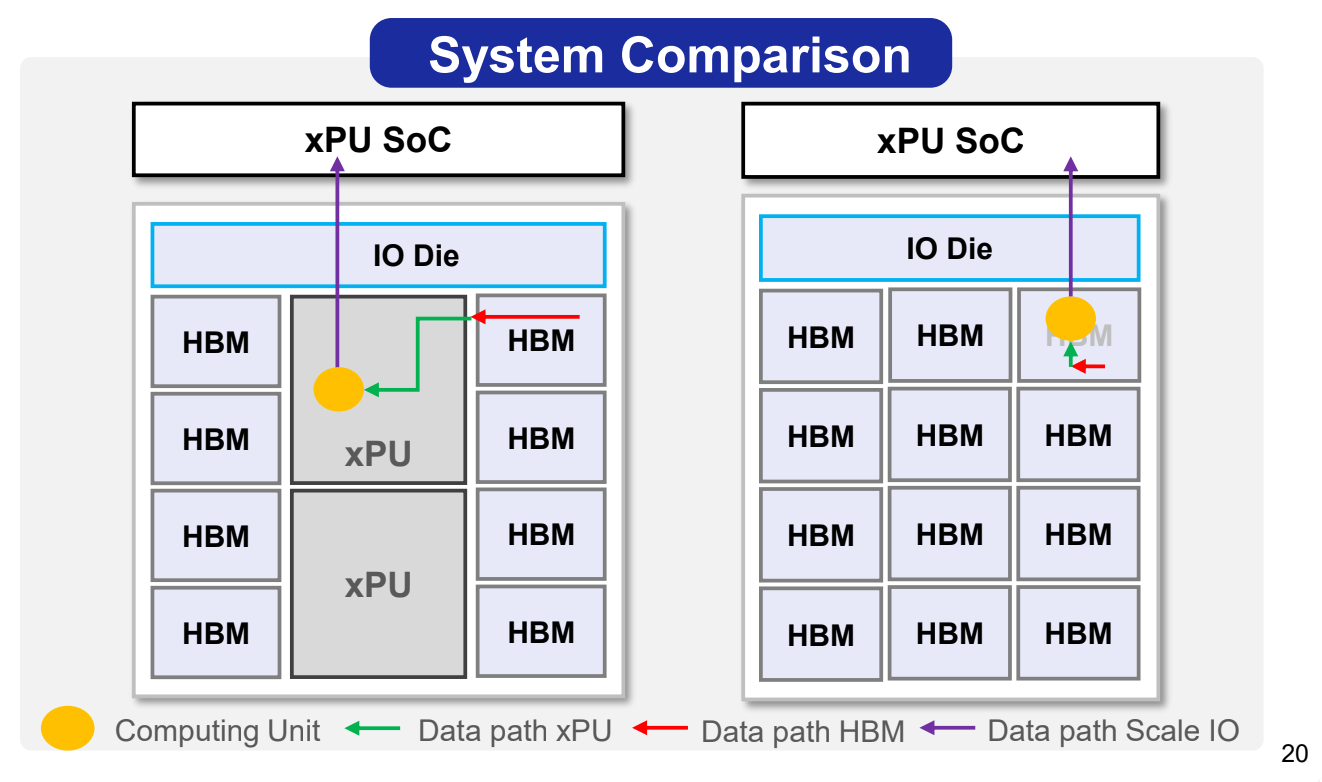
Finally, if logic transistors are available, then why not throw in some compute within the base die too? The benefit is that some compute like matrix compression or encoding can be done on the logic die without ever leaving this base die. This has latency and efficiency advantages.
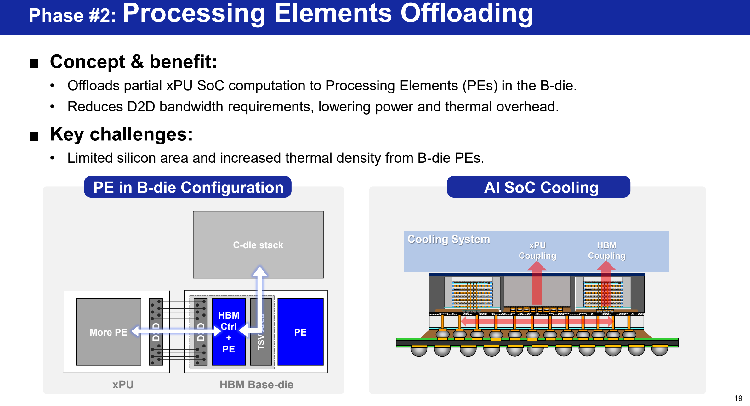
If that all works out, then one can in theory construct the nice little accelerator on the bottom right. It is easy to draw block diagrams like this, and conceptually nice to imagine, but its real performance benefits are questionable.
Phase 3: Going vertical
The final phase is use the custom base die + HBM and stack it on top of the logic die. The distance between compute and memory is short, and thus bits need to be shuffled across much shorter distances which gives power efficiency benefits and increased memory bandwidth due to the ability to use more parallel data paths across the chip area rather than just the beach front.
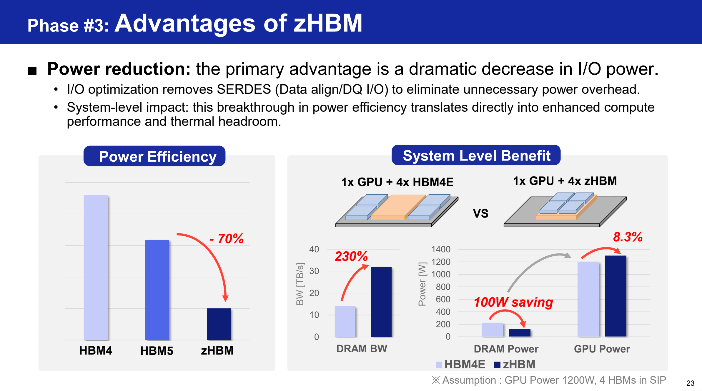
None of this is easy, but it is important for a company to have a roadmap ahead to improve technology. It proves that they have a path to an improved product in the future, and that is good to see in a company. Whether the market is ready to uptake that product is a different argument.
SK Hynix: MR-MUF advantage ends with Hybrid Bonding
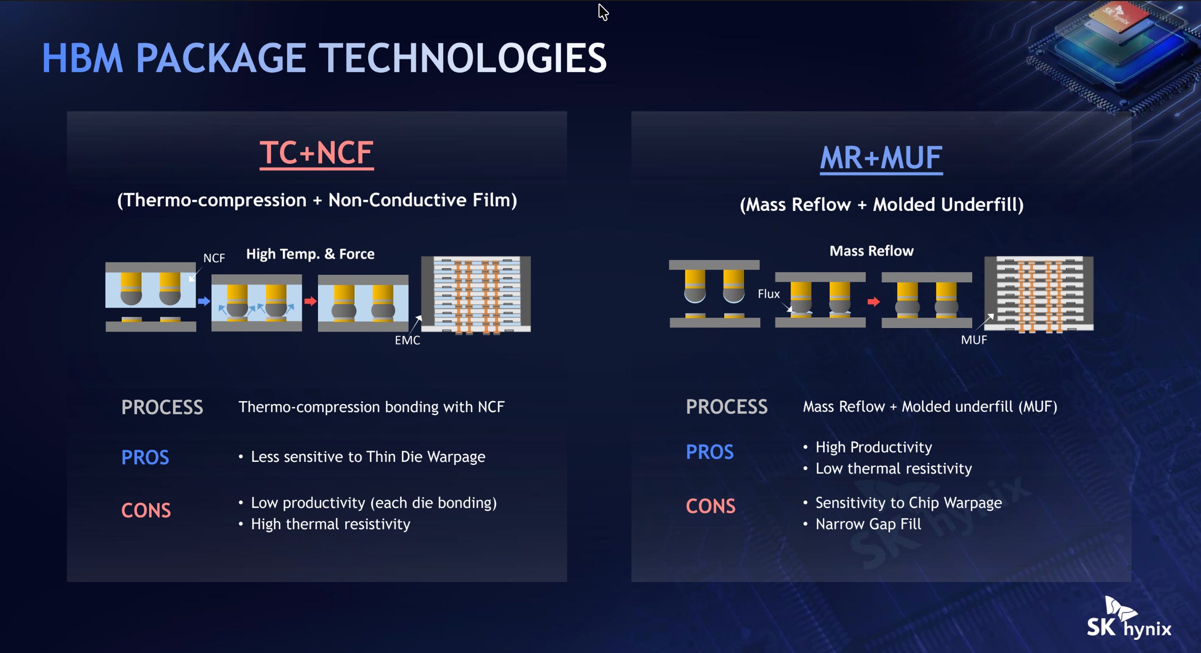
SK Hynix’s performance advantage in HBM has always been their use of Mass-Reflow Mold-UnderFill (MR-MUF) technique which provides them with a unique advantage over Thermo Compression Bonding (TCB) we have discussed in detail in the past on this newsletter.

The slide below from SK Hynix highlights this advantage.
In fact, they have no problem in boldly claiming that MRMUF method works well for 16-high HBM, but that it would require 775 microns of overall stack height. The JEDEC spec was actually revised to support the larger height, so it does add up.
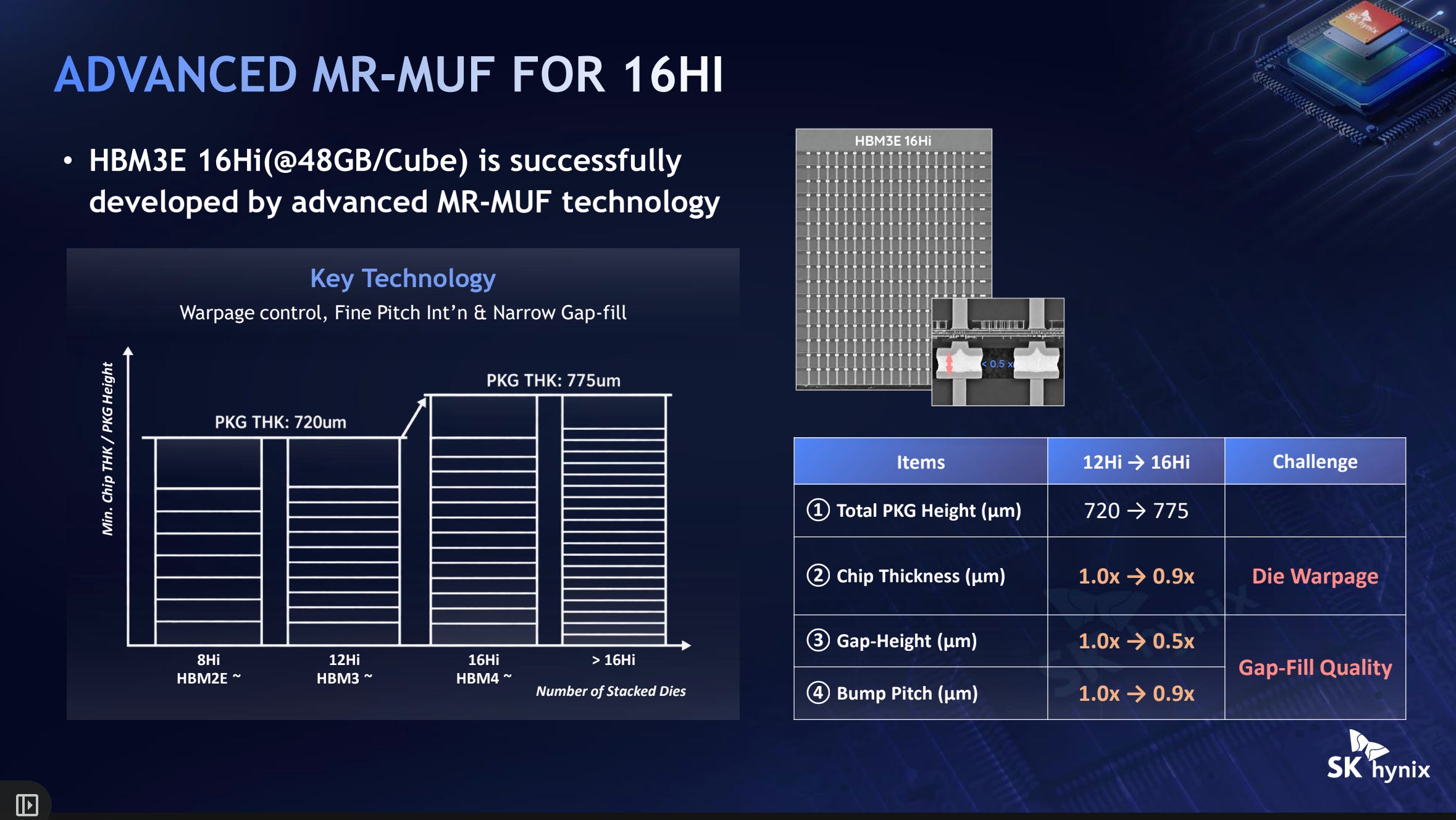
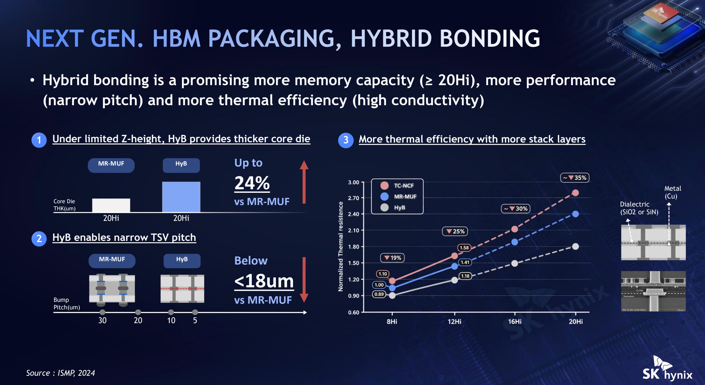
The question is: where does this MRMUF advantage go in the era of hybrid bonding, assuming that we ever get there and there is still a need for 20 high HBM.
Note that there is a chance that we will never get there because each DRAM wafer used for HBM purposes sucks up 3-4 times more wafers per bit. Given that the cost of memory alone is well above half the overall cost of a rack, the industry is trending to rely less on HBM if possible. This is where the news of de-specing HBM from 12-high to 8-high, and possibly even 4-high for some SKUs is coming from.
The slide below shows the benefit of MRMUF over TCB, where the thermal resistance is lower, and consequently results in better removal of heat from the middle regions of the stack. When hybrid bonding is used, the “secret sauce” of SK Hynix with MRMUF is no more, and everybody’s hybrid bonded HBM falls to the same level. If it comes down to this, it comes down to execution.
The thermal management slide from SK Hynix below has an unusual comparison table that shows how Micron is the only one without an external heat removal solution. Samsung has Heat Block Path (HPB), and SK Hynix has Integrated Cooling Enging (ICE). Micron is just going to “improve circuit design” to get there. If that were the case, Samsung and SK Hynix would be doing it too instead of external cooling blocks.
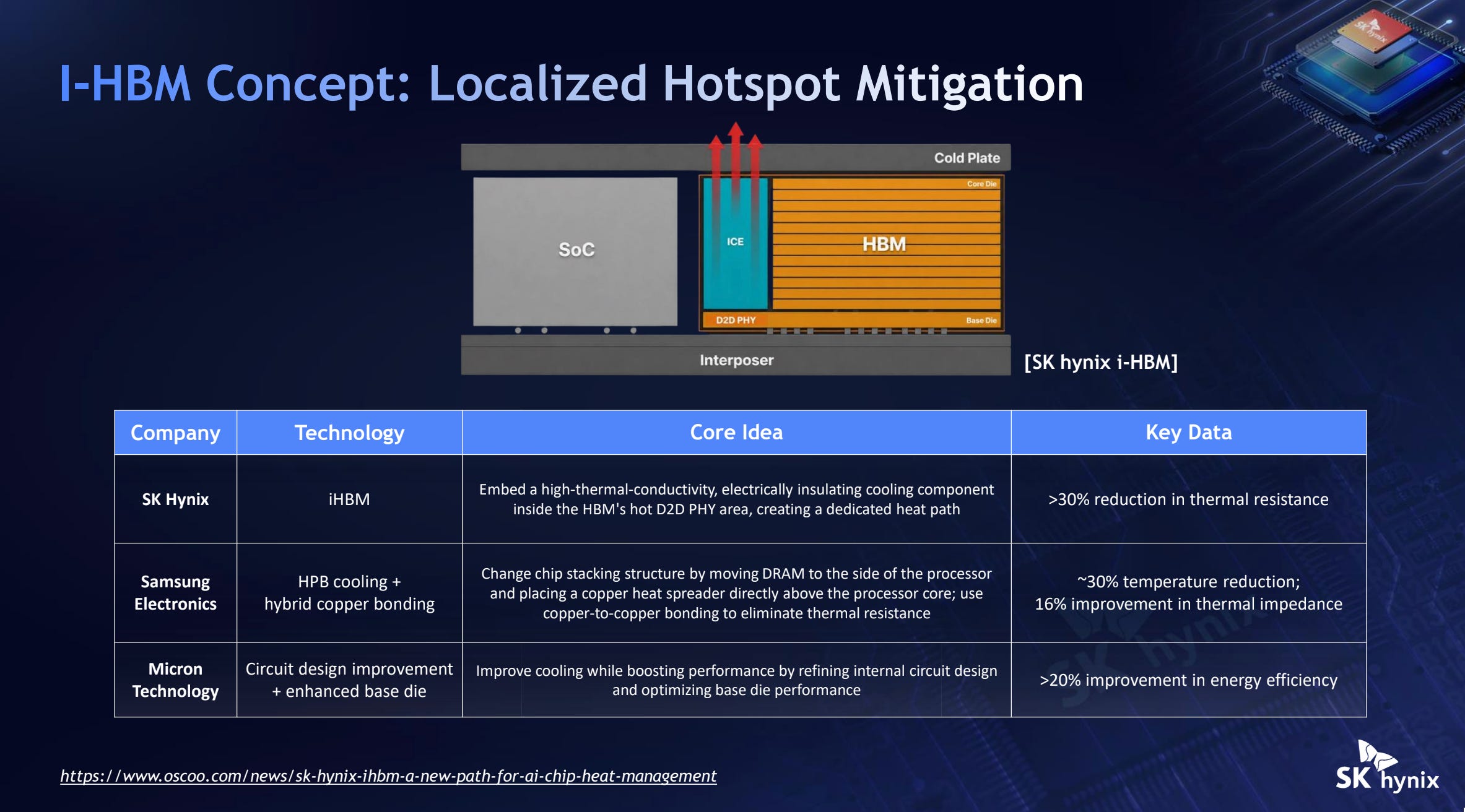
So it is either that Micron is behind on its next generation development, or has concluded that HBM will never reach those levels of stack height or per lane speeds that would require the development of advanced cooling solutions. It is not clear which one it is at the moment.
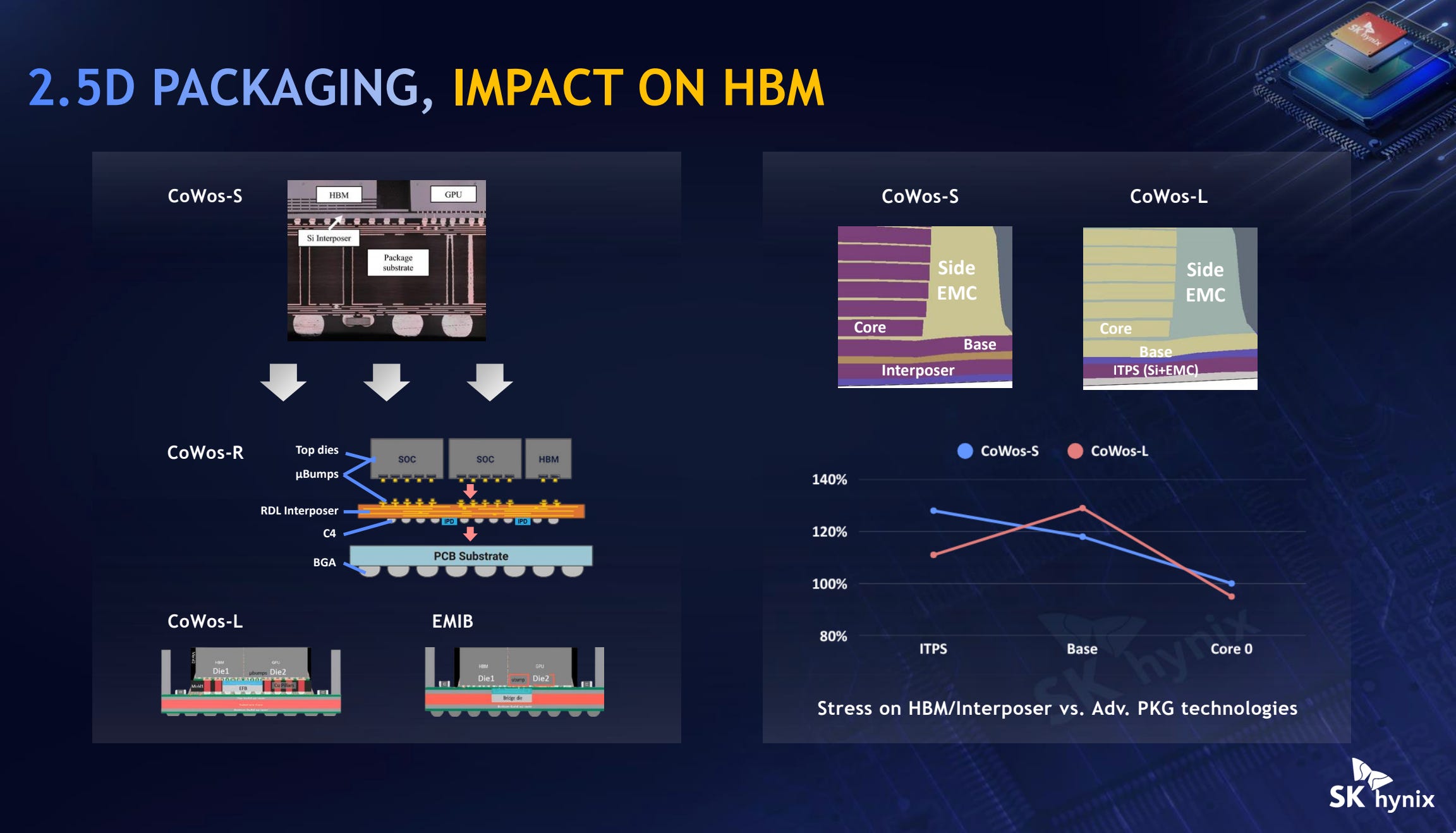
Lastly, there is an interesting mention on Intel’s EMIB on SK Hynix’s slide, noting that there are some customers using their memory with Intel’s packaging.
Final Thought
Even if stack heights do not go to 12, 16, or 20 in production environments, the use of custom base die on leading edge logic nodes is going to become important. It enables a higher data rate per pin, and we can see it being used even with lower stack heights due to all the advantages that Samsung pointed out.
The use of custom base die is, in a sense, decoupled from the stack height because it materially provides a plethora of advantages over a standard base die developed in a memory technology. In this regard, Samsung has the advantage in this playing field due to the availability of in-house advanced logic processes.
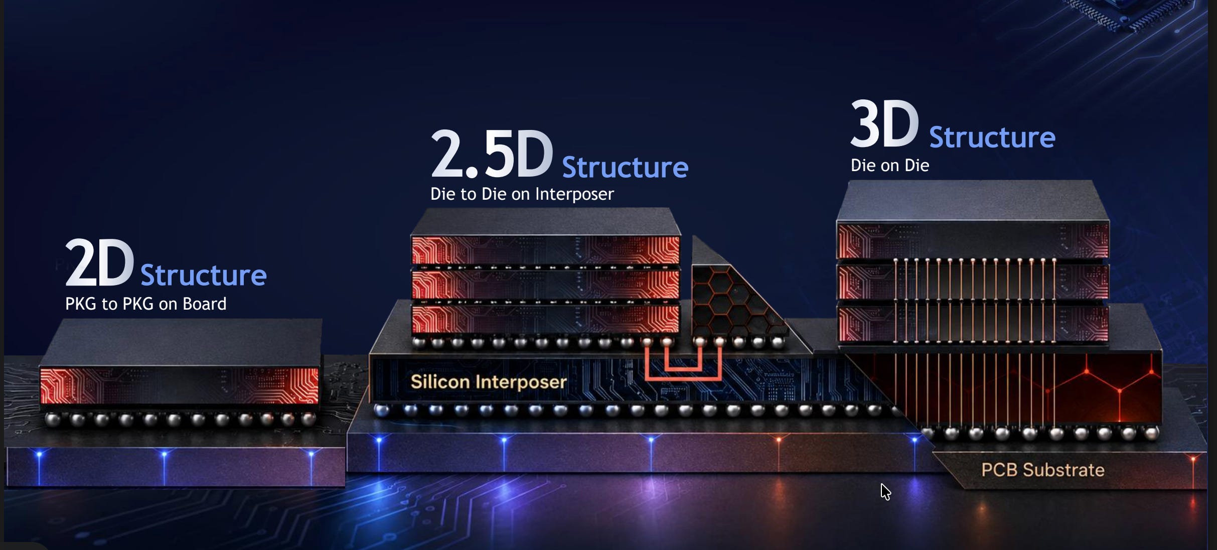
Lastly, I really love beautiful 3D renders of HBM sitting next to GPUs. SK Hynix’s look the best.
Thanks for making this free. I'm a personal investor but also excited about tech that wants to learn.
Appreciate you man!
Typo Also check out the Semi Doped podcast with and myself, and our daily free newsletter with latest semi news.