

A recent notable trend is that HBM performance is decoupling from stack height. Reports over the last month that Rubin Ultra drops HBM from 12-high to 8-high have been read as a supply/cost-driven downgrade, which is true. But the larger shift is that bandwidth, not capacity, is becoming the metric that matters in HBM. What sets HBM apart going forward is bandwidth performance via the custom base die, and value accrues to whoever designs it.
The industry is already treating capacity as a problem to route around rather than stack for. At Hot Chips, the sentiment among attendees was that high HBM stacks are too expensive and possibly unnecessary. Stacking higher was the brute-force approach but as memory costs rise, hardware builders are looking elsewhere for performance. This leaves memory makers with one remaining source of upside: 16/20-high hybrid bonding, the know-how only they hold. The despec trend is a direct risk to it.
This note covers:
The hard road to HBM bandwidth: A look back at the rocky path to achieving high pin speeds on HBM4, and what that has taught us about memory companies.
GDDR vs HBM: Memory companies know how to push GDDR lane speeds, but why HBM is different, and far more difficult.
NVHBM implications: Why things are changing when design experts on logic nodes take over critical parts of the HBM stack.
Where the value accrues: The rise of custom base die shifts where the value accrues in HBM, and where the pennies fall between memory companies and XPU builders.
Signals to watch and potential winners: The signs are already here, but what to watch for next, and who might emerge winners in the custom base die era.
By reading this post, you agree to the terms and conditions. See the full ethics statement.
If you’re new, check out the About page. A lot of readers expense the subscription to this newsletter as it helps their professional work. Group subscriptions (3+) are 20% off. If you have any questions, reply to this email and let me know!
Check out the Semi Doped podcast with and myself, and our daily free newsletter with latest semi news. For institutional research, contact SemiExponent.
The Hard Road to HBM Bandwidth
A keen observation that Tanj Bennett (Tanj) from SemiAnalysis made at Hot Chips was that memory makers are not concentrating on increasing bandwidth in HBM, but instead insist on stacking DRAM die. HBM4 already has 2,048 parallel data lanes, and packaging constraints makes it difficult to double that in the next generation. The better option is to increase the speed per lane. We have seen pin speeds in HBM4 being pushed from the 8 Gbps JEDEC spec, to 10 Gbps and beyond. HBM4e even pushes this to 16 Gbps.
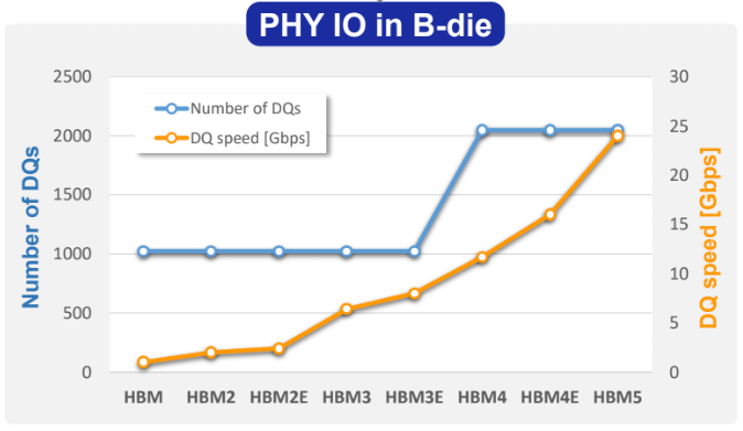
Source: Samsung, Hot Chips 2026.
However, asking a memory company to push lane speeds is like asking a penguin to fly. Memory companies have had boatloads of trouble with high-speed PHY design for HBM. Here is a brief history:
In the HBM3e era, Samsung struggled to pass qualification with NVIDIA due to a combination of yield, electrical and thermal issues. Things have notably turned around for Samsung when it comes to HBM4. Their in-house logic expertise at 4nm node provides an advantage in making high quality base die. They claim that they can push the speed to 13 Gbps per pin due to this choice.
SK Hynix has had significant problems with HBM4, and have allegedly caused delays in Rubin shipments. They used TSMC’s 12nm node for base die design in HBM4, and that choice has held them back from cutting edge lane speeds. It should however be sufficiently fast for current HBM deployments. SK Hynix is reportedly teaming up with Intel as a dual-source for next gen HBM base die. Our guess is that they will use Intel 3-T (Intel 3 with TSV) initially.
Micron has visibly been lagging at HBM4 due to their choice of DRAM-process node for the base die instead of a logic node. SemiAnalysis reported earlier this year that Micron’s share of HBM in Rubin would be zero for the first 12 months. This view seems to have changed since, with Micron getting qualified on Rubin along with SK Hynix and Samsung.
According to Counterpoint research, the current global HBM market share is led by SK Hynix, followed by equal shares between Samsung and Micron. SK Hynix has been NVIDIA’s largest supplier, and Samsung is gaining in Rubin allocations.
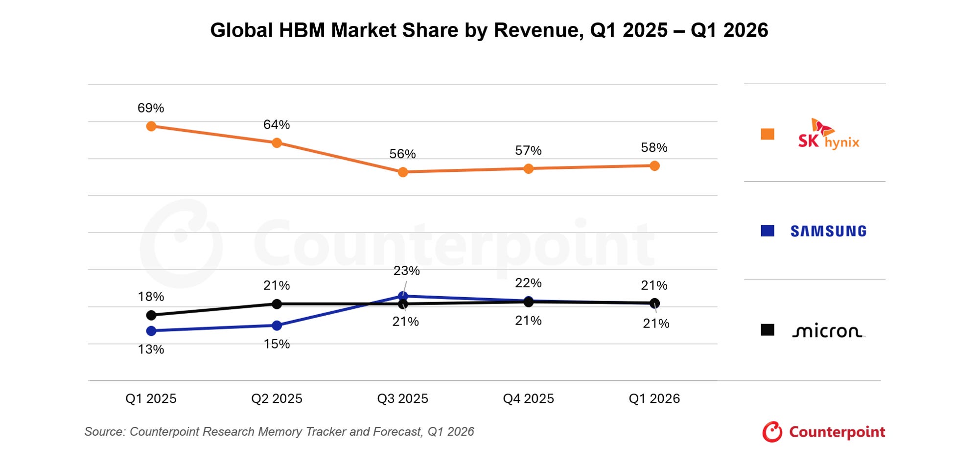
The market equilibrium HBM4 has reached is a consequence of fierce competition, delays, and fears of market share loss, where the supplier-buyer relationship has been tested several times over. Getting more HBM bandwidth means that amateur hour is over, and the value is going to tilt in the favor of those who know how to design high speed PHY links with logic nodes.
PHY Design: GDDR vs HBM
While memory companies have dealt with fast interface speeds in GDDR products, the difficulty in HBM is next level. It is important to understand the physics at play.
Bus width: GDDR7 relies on a 32-bit wide bus running at 48 Gbps per pin, but the fewer wires compared to HBM means that crosstalk is lesser, and heat is more distributed over the motherboard. HBM4 runs a 2,048-wide bus where the crosstalk between wires is much higher, and thermal dissipation is challenging.
PHY design: The circuits that push bits across a bus are substantially larger if they need to run fast, and consume more power. Circuit techniques to recover signal integrity at fast data rates are required like multilevel signalling, Decision Feedback Equalization (DFE) and Continuous Time Linear Equalization (CTLE), which takes physical space to implement (note: we explain this in simple terms on the Semi Doped podcast episode on Astera Labs retimers, if you are interested). Most of these techniques have become important at HBM3e and beyond as vendors push lane speeds, but are still vastly simplified compared to GDDR7.
The table below from Rambus shows the differences between GDDR6 and HBM2 design, as an example.
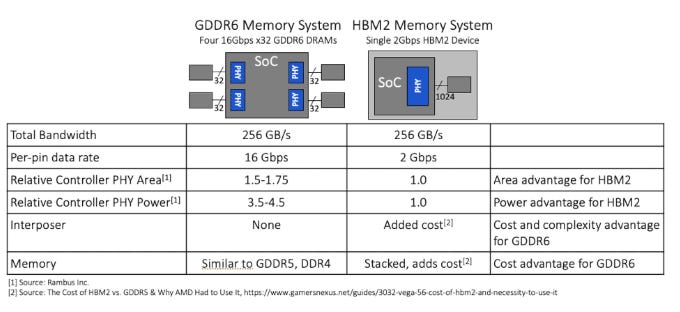
The need for HBM to work with XPUs in an unforgiving thermal environment while having strict performance requirements imposed by the likes of NVIDIA makes it challenging. While GDDR memory has been put into consumer graphics cards, the sheer scale of AI accelerators makes it a different problem – one that memory companies are not best poised to solve. Building faster PHY blocks in HBM for AI accelerators is arguably out of many memory companies’ core competence. Yet, this is exactly what the industry needs: better design of circuits on base die to push the performance.
NVHBM: Amateur Hour is Over
NVIDIA recently announced NVHBM, which they describe as:
“a custom HBM base-die technology designed and validated with leading memory vendors that enables increased memory bandwidth, better area savings, and lower power consumption.”
The implication of this announcement is much more significant than industry commentary realizes. As one X comment rightly put it, “base die is the Trojan horse into the memory industry.” So far, NVIDIA has had to live with the base die design choices made by memory companies, some of which are highly questionable as we discussed earlier. NVHBM is NVIDIA’s way of taking destiny into their own hands.
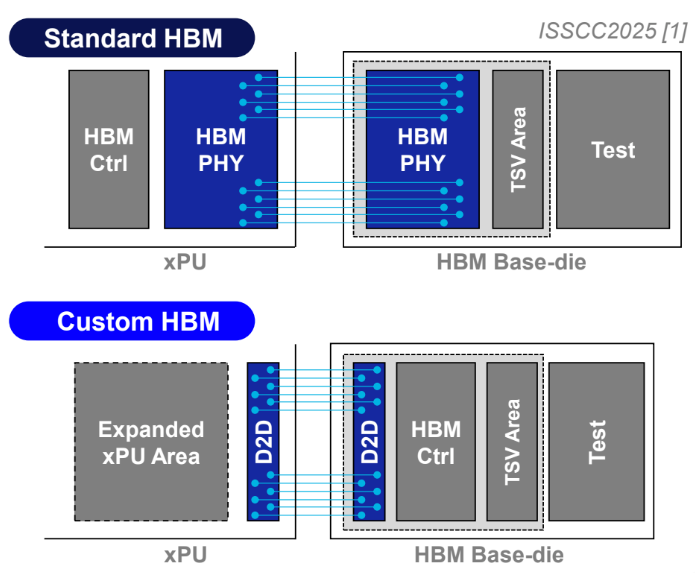
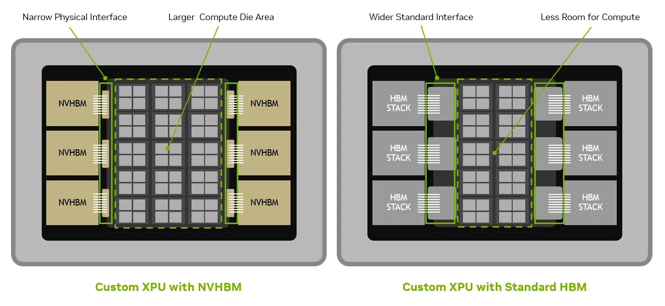
NVHBM moves the memory controller from the XPU to the custom base die, while the PHY interface itself is smaller on both the base die and the XPU. This picture from Samsung conveys how a good PHY design saves space on both the XPU and the custom base die.
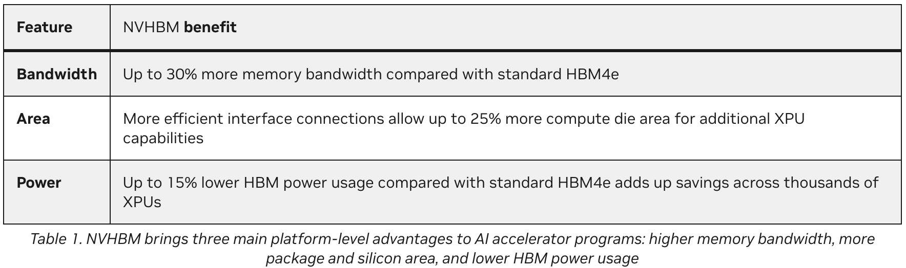
NVIDIA claims that NVHBM provides improved performance. Here is a table from their technical blog.
Source: NVIDIA
A 30% higher memory bandwidth than HBM4e, which would put the per pin rate at >20 Gbps while having 15% lower power usage. The smaller PHY design frees up additional space for more compute cores in the XPU die. NVIDIA’s blog shows how this works in a custom ASIC accelerator.
Source: NVIDIA
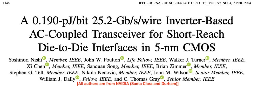
NVIDIA has actually published research in the Journal of Solid State Circuits on high-speed die-to-die interfaces where they demonstrated 25.2 Gbps/link at an energy efficiency of 0.19 pJ/bit over a 1.2mm link on TSMC 5nm. We won’t go into the technical details here, but the marketing specs around the NVHBM announcement seem feasible given their published work.
A custom base die design in the hands of a circuit design company such as NVIDIA, Broadcom, AMD, Marvell, or similar, would bring the world’s best PHY designers to the problem of increased HBM bandwidth. The co-design of the custom base die with the XPU opens up possibilities to push the performance even higher – a path we are just getting started on. If you want to understand more about what custom base die enables, see my free post from the Hot Chips memory tutorial below.
Hot Chips 2026: Tuning into Memory Vibes

This is my first time attending the Hot Chips conference and the overall vibe was a small, tight knit conference with a lot of interactions. No parallel tracks running and continuously having to choose what to attend. The talks from big companies, especially the big three, were pretty detailed; think of it as a collection of heavily technical keynotes.
Where Value Accrues in HBM
This question can be answered by examining where the boundary between HBM and XPU lies, and who is best positioned to provide what piece of hardware.
Beyond the paywall: where the value splits between base die and DRAM stack, why low-height HBM commoditizes, where memory makers' pricing power comes from, and who wins.