
How Dennard Scaling Allowed Transistors to Shrink
A detailed explanation of Robert Dennard's exact rules to scale a MOS-transistor's dimensions that resulted in more transistors on a single chip without any thermal penalty.

After watching Asianometry’s excellent video on the end of Dennard scaling, I took the time to dig into Robert Dennard’s original paper because it represents what engineers would call a ‘step function’ in the performance of a CMOS transistor.
To understand the significance of the original paper, imagine if someone wrote a paper explaining how Intel could have gone from the 10 nm node to the 2 nm node in one jump, eliminating elaborate scaling plans like 5YN4. This is what Dennard and his team showed in 1974. They demonstrated a transistor with 1 micron gate length, when everyone was at 5 microns. While not entirely the same, it was still an enormous leap in the evolution of the transistor.
Dennard scaling, in conjunction with Moore’s law, has been responsible for transistors getting faster over several decades since the inception of the transistor. Two decades ago, we hit the infamous “power-wall”, when Dennard Scaling ended. Nevertheless, it has gotten us to where we are today, and is worth looking back at.
Today, we will discuss the intricate details of Dennard Scaling:
A rapid primer on transistor operation
Structure of a 5 micron transistor
Issues with transistor shrink
Dennard’s Secret Sauce
Ion-Implantation under the Gate
Impact of Scaling on Circuit Performance
Interconnect Scaling Rules
Conclusion
Read time: 13 mins
This is a free article for the month, and please do consider upgrading to a paid subscription. It supports the writing of these posts, and paid subscribers get additional content, extended references, and a whole lot more.
Till January 14th, you can get a yearly subscription at $99/year instead of $150/year — a 34% discount for early supporters.
If you’re not ready yet, that’s totally cool! You can earn 1-month of paid subscription benefits by referring this publication to just two friends or colleagues!
A Rapid Primer on Transistor Operation
Before we can dive into how Dennard’s paper changed everything, we need at least a basic understanding of transistor operation and its limitations. So we will only cover exactly what is sufficient to understand Dennard scaling, and use a lot of pictures. If you’re already familiar with transistor operation, skip ahead.
A transistor has a gate terminal which controls the flow of electrons from source to drain, through a silicon channel. The gate is usually made of polycrystalline silicon and is separated from the actual bulk silicon channel by a layer of silicon dioxide, which acts as an insulator. The source and drain regions are usually heavily loaded with electrons by a process called doping. The bulk silicon surrounding the source/drain regions where the channel is formed is called the body of the transistor, and also doped but less heavily so.

When the gate voltage is above a certain value called threshold voltage, it transfers copious amounts of electrons from source to drain via a conducting channel that forms in the silicon. When below threshold voltage, most of the current is prevented from flowing from source to drain, but some accidentally leaks through. The length of the gate polysilicon dictates how far the source and drain are from each other. The closer they are, the quicker electrons get from source to drain, and the faster the transistor can switch. We always want smaller gate length. A voltage applied to the body can alter the threshold voltage of a transistor through a mechanism called back-gate bias, or is often also called the body effect.

When a voltage is applied to the source and drain regions, the bulk silicon around the source and drain get depleted of charges. This is because the source/drain and bulk are doped with charge carriers that have opposite signs which neutralize in the region immediately surrounding the implanted regions. The width of the depletion regions depends on the doping level — the higher the doping, the smaller the depletion width because the neutralizing charge is more easily available.
When the depleted regions get closer together, the transistor’s threshold voltage changes. This is called short-channel effect, and is a phenomenon that plagues smaller transistors. As the drain terminal voltage increases, the threshold voltage of the transistor is further lowered through an effect called drain-induced barrier lowering (DIBL). We won’t get into why these things happen; it is sufficient to know it does.
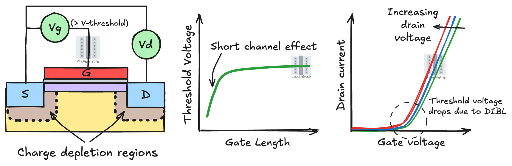
We must also remember that the transistor does not suddenly turn off when gate voltage goes below threshold. Instead, it starts to conduct orders of magnitude lower current and the actual value at a gate voltage corresponding to the off condition depends on how fast the current drops as voltage is dropped below threshold. This rate of current drop when below threshold voltage is called sub-threshold slope. We want a high sub-threshold slope so that there is minimal leakage when the transistor is off. Since, body effect and DIBL affect threshold voltage, they also affect how much off state leakage is present in a transistor, and is therefore considered important.

Here is a quick summary of the terms described, should you need to refer to them through the rest of this article:
Gate length: The actual length of the polycrystalline silicon used as gate, or you can loosely think of it as the separation between source and drain terminals. Smaller the length, faster the transistor.
Threshold voltage: The voltage at the gate that turns the transistor on or off.
Short-channel effect: As gate length shrinks, threshold voltage drops due to the proximity of the charge depletion regions around source and drain.
Body effect: The application of voltage to the body of the transistor affects the threshold voltage of the transistor.
Drain-induced barrier lowering (DIBL): The increase of voltage on the drain lowers the threshold voltage depending on the construction of the transistor.
Sub-threshold slope: The rate at which current drops off when gate voltage is below threshold. We like high slopes.
That should do. Now we can talk about transistor scaling.
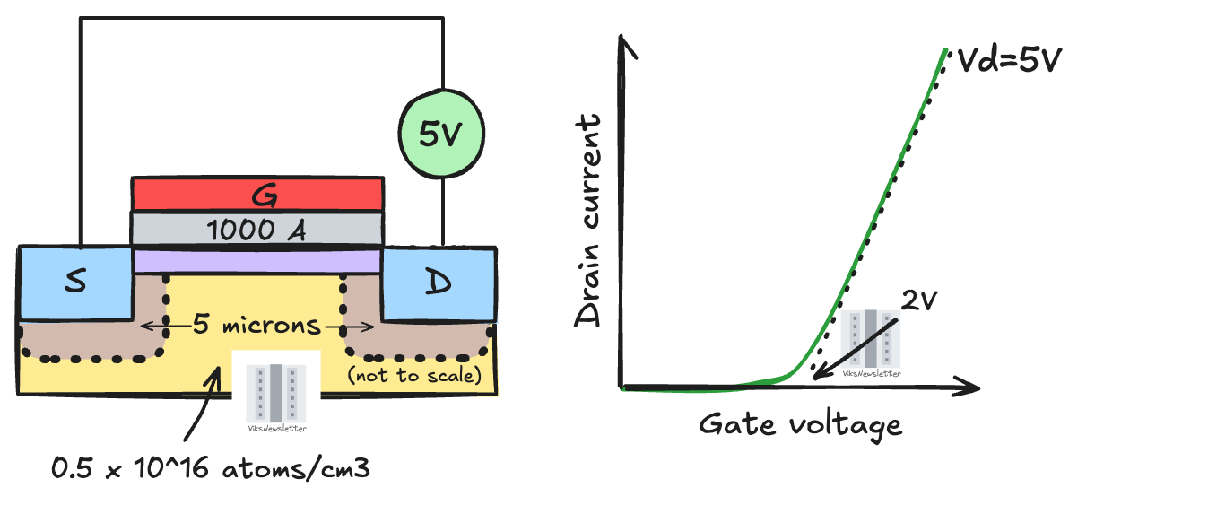
Structure of a 5 micron transistor
The 5 micron gate length transistor shown below reasonably represents what was considered a ‘state-of-the-art’ transistor in the early 1970s. The gate oxide thickness was 1000 angstroms (or 0.1 micron, or 100 nm). The transistor threshold voltage was about 2V, and it was operated as a switch using a 5V drain supply voltage. The silicon substrate doping was kept low enough at 0.5x10^16 atoms/cm3, which kept the body effect in check by not allowing too much variation of threshold voltage with body bias1.
Issues with transistor shrink
If this transistor gate length is made a factor of K (say K=5) times smaller, then it is apparent that the depletion regions around the source and drain would touch. Then there would be no conduction channel, and hence no transistor operation.

Even if this were not an issue, putting 5 volts across the drain but reducing the channel length by 5x increases the electric field by a factor of five (electric field is the voltage difference between source and drain divided by the distance between them.) High electric fields cause the transistor and its associated semiconductor junctions to breakdown and get damaged.
Dennard’s Secret Sauce
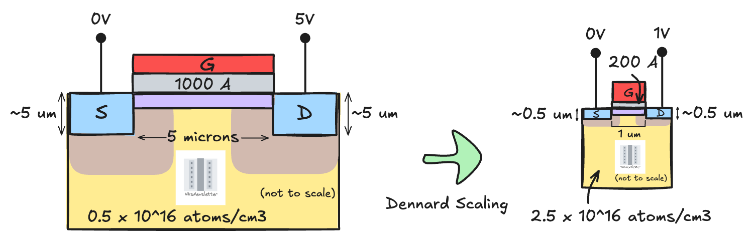
Dennard suggested that the transistor be adjusted in three ways:
Dimensions: Scale down all linear dimensions by a factor of K. When the gate length is reduced by K, the gate oxide thickness, implanted source/drain depth, and transistor width (the dimension of the transistor going into or out of the page) should all be reduced by the same factor.
Voltage: Reduce the voltage applied to the device by a factor of K. If the voltage is reduced as the dimensions shrink, then the electric field can be kept constant. The threshold voltage also scales by a factor of K when the gate oxide thickness is scaled down so that the transistor operates at reduced drain voltages.
Doping: Increase body doping concentration by a factor of K. By increasing the substrate doping, the depletion widths can be reduced by the same factor which is important to keep them from touching each other.
All these modifications cause the drain current of the transistor to also drop by a factor of K. Since the electric field in the channel is unchanged after the shrink, the qualitative behavior of the smaller transistor would remain unchanged.
When Dennard and his team implemented these scaling rules in an experimental transistor and tested it, they found that the current and voltage scaled almost perfectly. The threshold voltages had scaled down a factor of five too. The theory of device scaling worked perfectly to a level that surprised Dennard himself, who wrote,
… the exact match on the current scale is thought to be fortuitous since there is some experimental uncertainty in the magnitude of the channel length used to normalize the characteristics …

There is however one parameter that does not scale — the sub-threshold slope, which Dennard in his seminal paper pointed out by writing,
In order to design devices for operation at room temperature and above, one must accept the fact that the subthreshold behavior does not scale as desired.
This as it turns out would be one of the contributing factors to the eventual end of Dennard scaling in transistors thirty years later. As transistors scaled down, the leakage current of transistors which were in the off-state resulted in increased current consumption and power dissipation, without providing any meaningful improvement in clock speeds. We will briefly return to this point later in this article.
The diagram below compares the transistor dimensions before and after the shrink as proposed by Dennard. While gate length is shorter, here are some other key observations to be made in the smaller transistor (all in accordance with the principles we laid out earlier):
Gate oxide is thinner (200A vs 1000A)
Source/drain junction depths are shallower (0.5um vs 5um)
Body doping is heavier (2.5x10^16 vs 0.5x10^16)
Drain voltage is lower (1V vs 5V)
Ion-Implantation under the Gate
Dennard also explained in his paper that the dopants added to form the source, drain, channel and body should be properly engineered to squeeze performance from the transistor. He described this as the process of ion-implantation which is a major part of the original paper, but is often not mentioned when Dennard Scaling is discussed.
While the scaled device structure provided good performance, improvements can be made to the conducting channel region right under the gate. The process of ion-implantation involves adding a higher dopant concentration right under the gate region, and subsequently lowering the doping concentration of the substrate body.

The purpose of doing this is to make the depletion region extend more vertically under the drain region, rather than extend under the gate, under the influence of a voltage at the drain. This would allow better threshold voltage control as the device is scaled, and improved operation of the transistor. Due to higher separation between depletion regions of source and drain, the device capacitance is also reduced, which allows for higher switching speed.
Due to better gate control, the gate oxide thickness could be increased from 200A to 350A without degrading threshold voltage of the device. A thicker gate oxide provided better device reliability, at least using the manufacturing processes available at the time.
Impact of Scaling on Circuit Performance
The table below, derived from Dennard’s original paper, shows the impact of scaling on various circuit parameters.
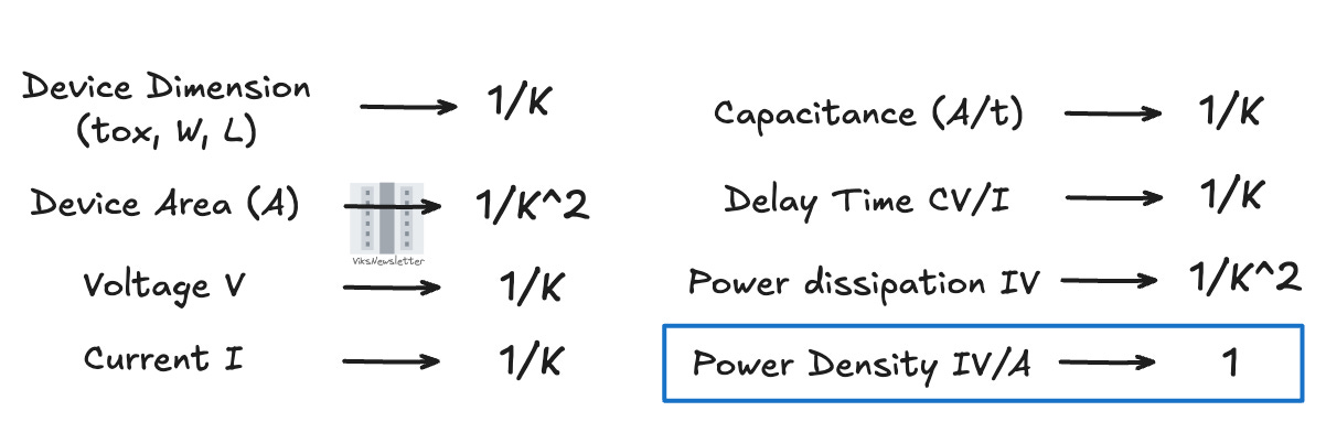
The most important aspect of Dennard Scaling, which almost everyone refers to when talking about shrinking transistor dimensions is the power density being constant.
Dennard Scaling shows that more transistors can be placed on a chip while the thermal dissipation remains unchanged.
This result is so important, we’ll say it another way.
When coupled with Moore’s law which states that the number of transistors on a chip will double every two years, Dennard Scaling states that the increase in transistor count comes with no thermal penalty.
The phenomenon of ‘yes, there is free lunch’ comes ever so rarely in engineering. The ability to build more transistors in a chip without having to worry about cooling accelerated the availability of compute power for many decades, and is solely responsible for the rapid development of chip technology in the past century.
An added benefit comes from the drop in delay time by a factor of 1/K which means that not only were we able to cram in more transistors with no thermal penalty, but those transistors switched faster too, enabling higher clock speeds. This really is an instance of ‘having your cake and eating it too.’
Interconnect Scaling Rules
An often overlooked aspect of Dennard Scaling is how interconnects scale as transistors shrink. As transistors get smaller, the metal lines that connect to them have to shrink too, as we saw in an earlier post on the need for ruthenium interconnects. The scaling of the transistor has the following implications on interconnect performance.
Resistance: If the dimension along one direction such transistor width decreases by K, the line widths have to shrink by the same factor to connect to it. This means that the line resistance also increases by a factor of K, assuming line thickness is unchanged (and that the width is not of the order of mean free path.)
Normalized IR drop (IR/V): When the resistance increases K-times, the current which has scaled 1/K-times causes the same voltage drop as the unscaled transistor. However, this voltage drop has greater implications for the smaller transistor which already uses a lower supply voltage. This means that the ‘normalized’ voltage drop increases K-times due to current flowing through thin metal lines.
Interconnect delay (RC): If resistance increases K-times and capacitance of the transistor scales by 1/K, the interconnect delay is essentially unchanged. While this may seem like a good thing, it is actually a downside because a smaller transistor switches faster and needs lower interconnect delay. An unchanged delay means that the interconnect is a greater obstacle for a smaller transistor.
Current density (I/A): Current density in a scaled-down conductor is K-times higher and may actually pose a reliability risk due to electromigration concerns.
In all, the interconnect scaling rules can be summarized according to the table below.

Conclusions
The scaling rules outlined by Dennard and his team served for over 30 years, providing faster single transistor clock speeds while the transistor count kept increasing. Right around 2005, when gate length reached 90 nm or thereabouts, Dennard scaling ended. Shrinking transistor dimensions further did not increase the speed of the transistor. This is commonly referred to as the ‘power-wall.’
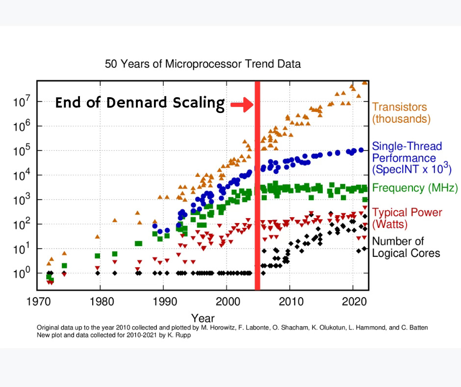
The power consumption of the chip rapidly increased resulting in thermal dissipation issues, without any performance benefit. Parts of the chip had to be turned off to manage thermal issues which came to be called ‘dark-silicon.’ Right around that time, the industry switched to multi-core architectures to keep Moore’s law going.
Today, transistor scaling has taken an entirely new trajectory in the post-Dennard world. We don’t rely on single-core clock frequencies anymore, but instead look at entire data centers as the new unit of compute. Modern transistor architectures rely on new materials, advanced physical architectures like FinFET and Gate-All-Around, or innovations at the system level to advance along Moore’s law of scaling.
Dennard Scaling is still an important piece of semiconductor and computer history that has enabled the world as we know it.
References
[1] R. H. Dennard, F. H. Gaensslen, H.-N. Yu, V. L. Rideout, E. Bassous, and A. R. LeBlanc, “Design of ion-implanted MOSFET’s with very small physical dimensions,” IEEE J. Solid-State Circuits, vol. 9, no. 5, pp. 256–268, Oct. 1974.
The views, thoughts, and opinions expressed in this newsletter are solely mine; they do not reflect the views or positions of my employer or any entities I am affiliated with. The content provided is for informational purposes only and does not constitute professional or investment advice.
For certain digital circuits like source followers, too much variation of threshold voltage is an issue resulting in incorrect circuit operation.
Lucid! I had not previously noticed the problem of decreasing gate voltage colliding with immovable sub threshold slope as one of the reasons scaling ended. Interesting that several limits all coincided about the same scale.
Carver Mead in the mid-1960s presented a comprehensive description of scaling of semiconductor devices, and published a prediction for sub-micron devices (expected as the limit to lithography), Dennard reduced that general case to a concise set of rules just for CMOS which provided a road ahead with constant power per area that everyone could drive. Sometimes less is Moore.
Thanks Vikram! In addition to the points you covered here so nicely, another factor that prevents true Dennard scaling are the quantum mechanical phenomena, especially tunneling, that become more and more important (likely) as the distances gating current flows decrease. Once we approached a gate thickness measured in nanometers, leak currents become significant. All this is in addition to the difficulty providing power through more and ever-smaller vias and the other factors you already described. All these factors contribute to more heat, something semiconductors especially at nanometer scale really don't like.
To go back to concrete examples: Intel's Pentium IV marked, IMHO, a true "hard stop" in their quest to keep increasing frequencies. The idea of having the CPU performing more and more tasks by few ( first one, later two) cores by running a core really, really fast hit a wall. With the Pentium IV, that wasn't helped by a design with a very long pipeline that caused trouble when it stalled. Which happened often enough. The entire industry then turned to multiple core designs and increasing speed and efficiency by including specialized circuitry (SIMDs) in the cores.