

In a July 6 X post, SemiAnalysis reported that Nvidia’s Kyber NVL144 rack has slipped by more than 12 months, from 2027 to 2028, because the PCB midplane remains hard to manufacture. Nvidia has pushed back saying that the roadmap is unchanged. A lot of the discourse is analyst sourced, and thus opinionated, including this note itself. I noted in an earlier X post that Nvidia’s moves all point to difficulty in copper scale-up for Kyber, which is why they were pushing for optical approaches.
Beyond the midplane PCB, SemiAnalysis notes that:
The NVL576 multi-rack system is also likely delayed or limited to small volumes due to CPO challenges, leaving Nvidia without a proven way to expand the scale-up world size for Rubin Ultra.
The NVL72x2 back-to-back architecture was cancelled after pushback from hyperscalers over its odd design and operational burden.
The Oberon rack will remain the mainstay, and Nvidia will sell more of them in the Rubin era to cover the Kyber shortfall. SemiAnalysis still sees data center compute revenue running 20 percent above consensus in the second half of FY27, so views are not uniformly bearish.
In this post, we will view all these claims through an engineering lens to understand the underlying physics, draw conclusions where possible, and suggest solutions that might be deployed.
Table of contents:
Is the midplane PCB really too hard to manufacture?
NVL72x2: Why It Might Have Really Been Cancelled
NVL72x2: How to Make it Work
CPO for Scaling up World Size
Does this really create an opening for Google and AMD?
At the end of this post, you will walk away with greater nuance as to what roadblocks are in the way of next generation hardware, how the big players are working around them, and where the pieces might fall in the future.
By reading this post, you agree to the terms and conditions. Also see the full ethics statement.
You can find the whole catalog of articles for purchase at this link. This article will be available for paid digital download shortly after publication.
This is how we think about market claims at SemiExponent. If you have a bet you'd like tested this way privately, get in touch.
Is the midplane PCB really too hard to manufacture?
Let’s first introduce the midplane PCB and explain what problem it aims to solve. Here is a picture of it:
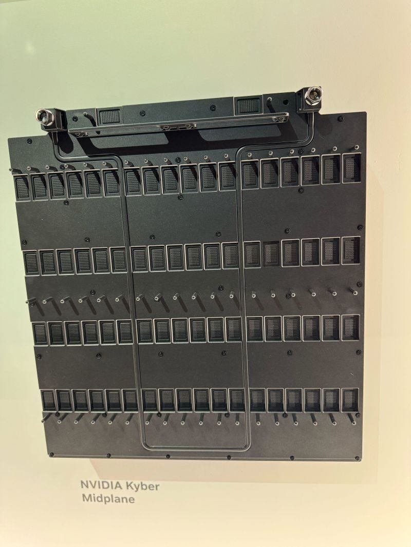
In all the generations of racks till date, the scale-up domain in NVIDIA racks has always been copper. There is a cable cartridge that contains just over 5,000 passive copper cables that hook up the GPUs in an all-to-all configuration. As the interconnect speeds in the scale-up domain increased in every successive generation, copper interconnect reach became an issue. Copper’s losses meant that you needed something much shorter than long copper cables running through a spine. Enter the PCB.
The idea of the PCB was simple: hook up all the GPUs and network switches on a board level, instead of cables running through a spine. The compute trays would hook into one side and the network switches on the other. Then, by simply running traces on the PCB, you can get GPUs hooked up to each other. Simple and elegant right?
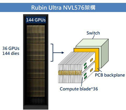
No. Turns out that this is a routing problem of gargantuan proportions (literally) because you can’t just draw metal lines between GPUs like in a picture. As a result the routing problem only increases. You would need to route over or under metal connections to prevent them from intersecting.
Think of a freeway intersection: to keep the flow of traffic moving smoothly, you have different levels of roads, each level adding a significant amount of complexity to the routing problem.

It’s the same problem on the PCB, except that you have about 78 layers. In addition, the Kyber rack has 144 GPUs compared to the Blackwell era “Oberon” rack which has 72 GPUs. The exact PCB layer count seems to differ based on who you ask, but the takeaway remains: it is a very complex PCB. The midplane PCB makes the equivalent of 20,000 connections that would otherwise need to be copper cables which would be too many to fit in the spine. These boards are built on separate 26 layer boards each nearly a square meter in size and then laminated together to form a massive PCB required for Kyber midplane.
Anybody who has worked with high speed interconnects knows that PCBs are not automatically better. Sure, you can pack a higher routing density in a smaller space cutting the reach distance, but that says nothing about the losses. In general cables have lower losses for high speed signals than metal lines on a PCB. To keep the midplane PCB losses in check, it is built on an advanced high-frequency material consisting of an M9-grade copper clad laminate (CCL) with Quartz glass (Q-glass) reinforcement. The use of these specific materials is so that the dissipation factor (~0.0007) is as low as possible. Dissipation factor is a measure of how much of the signal is lost in the PCB dielectric material. When you have so many layers, it is best to lose as little as possible.
The sheer size, number of layers, and specialized materials required for the midplane PCB make it an engineering marvel. When deploying this in production, the yield of the PCB and reliability in the field have to be exceptionally high. The obstacles are plenty:
No de-lamination can occur at any layer across a panel near a square meter.
Quartz glass is abrasive and hard to drill cleanly; connections between layers (through what are called vias) and drill bit wear become yield limiters.
Since yield compounds per layer, it becomes extremely difficult at 78 layers. A defect anywhere scraps the whole board.
A board-level failure affects the operation of 144 GPUs (in an NVL144 configuration) all at once.
These factors make the engineering marvel hard to build in volume. The reason we examined the underlying engineering is to ground rumors of schedule delays in engineering reality. Yes, building these boards is hard but not impossible. AI PCBs already span tens of layers easily, the midplane PCB takes it to another level.
Confirming or denying the delay outright requires tracking the supply chain and orders closely, which is out of scope here. Additionally, Nvidia has responded saying that their roadmap is intact – so we’ll take their word for it. But, if you are NVIDIA, and your best engineers say that the midplane PCB is hard, what’s the backup plan? The answer is the NVL72x2.
NVL72x2: Why It Might Have Really Been Cancelled
144 GPUs are difficult to fit into a rack for a couple of reasons:
They draw a lot more power per rack which would require the use of 800V DC systems to handle the power distribution and copper cable weight within the rack (see earlier detailed post on this below)
The routing problem as we discussed is complex, and requires an enormous PCB that is hard to make.
Power Delivery As The Next Physics Wall In AI Datacenters

One of the easier architectural changes to spot in AI datacenters are those that are physics-driven. Just like how copper interconnect reach was ultimately limited by losses, power delivery has a remarkably similar constraint: resistance.
The logical stopgap solution would be to instead put in 72 GPUs per rack, just like in the Blackwell era, and put in two such parallel racks back-to-back. This solves the scale-up interconnect problem within a rack because you only need to connect 72 GPUs in the rack just like in the Blackwell “Oberon” rack. NVIDIA can simply use existing racks and not have to worry about it. The 144 GPU implementation would then involve putting two such racks together.
The problem now is how to connect the two racks together so that they behave as if they were one rack.
While the Kyber issues were being sorted out, SemiAnalysis stated that NVIDIA considered a back-to-back configuration as shown below. Perhaps this configuration was known to their institutional clients, but a detailed check of my SemiAnalysis newsletter archives shows that this was not mentioned anywhere before – including in their Vera Rubin deep-dive. Perhaps it was not in consideration at the time of writing.
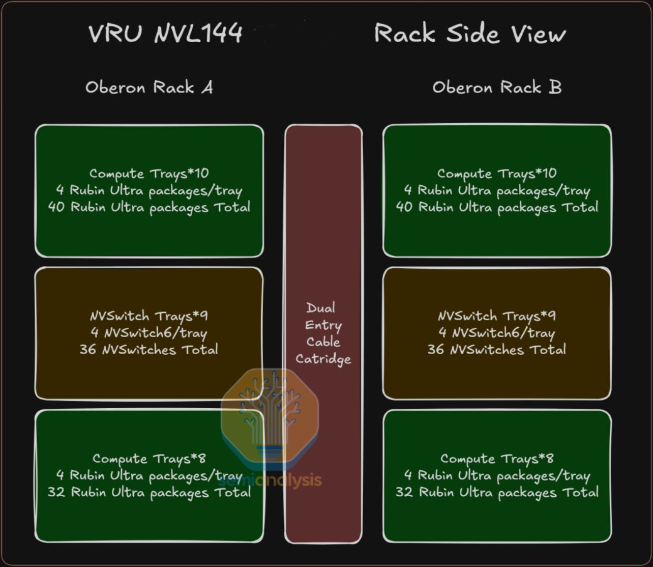
Regardless, this configuration was allegedly disliked by the hyperscalers for its “odd” configuration. This argument I do buy because the data halls are not laid out to accommodate racks in any orientation. There are cable raceways, cooling, and power all laid out to accommodate racks in a particular orientation, and going back-to-back will require changing all the data hall infrastructure. If this was actually suggested by Nvidia as a configuration, no wonder hyperscalers and CSPs pushed back. SemiAnalysis stated in their tweet that this configuration was cancelled.
However that does not mean the NVL72x2 will never work, or that there aren’t other ways around current challenges. Beyond the paywall, we discuss:
How to make the NVL72x2 work
Why CPO/NPO is the right answer for scaling to larger world size
Does this really create an opening for AMD and Google?