
Role of Storage in AI, Primer on NAND Flash, and Deep-Dive into QLC SSDs
A detailed look at how data moves through AI infrastructure - from HBM to SSD/HDD; how NAND flash works; the emerging role and challenges of high capacity QLC NAND flash SSDs for AI workloads.

Welcome to a 🔒 subscriber-only deep-dive edition 🔒 of my weekly newsletter. Each week, I help investors, professionals and students stay up-to-date on complex topics, and navigate the semiconductor industry.
If you’re new, start here. As a paid subscriber, you will get additional in-depth content. See here for all the benefits of upgrading your subscription tier!
Note to paid subscribers: This post is long, and to save you time, here is an executive summary post. Thanks for all your support! I still recommend reading the full post for a comprehensive understanding.

I have a video version, if you want to understand the fundamentals of NAND flash!
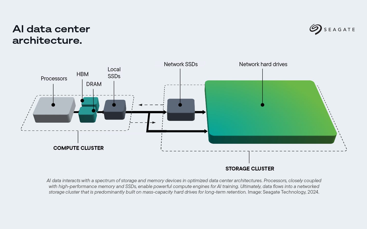
A lot of attention is given to compute, memory and networking in an AI data center - from how quickly GPUs get data from HBM, to how fast the interconnects in a datacenter are. What gets less attention is the design of high capacity storage for AI workloads.
Frontier models are trained on tens of trillions of tokens, which typically occupy multiple terabytes of training data depending on the precision format used. During the training process, voluminous amounts of data need to be delivered to the GPU on time for computation because underutilizing GPU time quickly adds to model training costs.
The storage demands on the inference side are even higher. With 800 million ChatGPT users and counting, all the queries, documents, images, and videos generated or uploaded need to be stored somewhere, and query results must be generated in a matter of milliseconds, or a few seconds at most. This requires in the range of 50-100 petabytes (1 PB = 1,000 TB) in a single storage rack.
All these workloads require fast access to high capacity storage, which is present as local SSDs within the compute tray, networked SSDs in a storage server connected over fabrics like Ethernet/Infiniband, or just massive clusters of HDDs for long term archival as shown in the picture below.
In this article, we will look at how data flows during training and inference, understand storage hierarchies in a datacenter, develop a thorough understanding of NAND flash technologies, and discuss emerging QLC NAND flash in quite some detail.
For free subscribers:
Role of Storage in LLMs: How the interplay between HBM and SSDs is essential to training and inference.
Storage hierarchy in AI datacenters: Understanding the cost, capacity and speed constraints of various storage devices.
Basic types of NAND cells: Floating gate and charge trap cells in NAND flash.
Single layer cell (SLC) flash: Operating principles behind the most basic form of flash.
Higher level cells (MLC, TLC, QLC): Expanding storage density by having more charge levels stored.
🔒 For paid subscribers:
Latency issues in multi-level NAND cells: Root causes for why higher capacity comes at the cost of higher latency.
Endurance and thermal stability: Fundamental reasons why the multi-level approach results in lower endurance, and also higher sensitivity to temperature.
QLC SSDs for AI workloads: Why this class of SSDs offer incredible storage density, and where it fits compared to HDDs, and TLC SSDs.
CPU requirements for QLC SSDs: Compute requirements when QLC SSDs are used in storage servers.
Testing challenges for QLC SSDs: What the fundamental constraints are in performance testing.
QLC adoption vs HDDs: What the advent of QLC-based storage systems means for HDD storage.
Market players: A quick rundown of all the competitors on the NAND SSD stage, their market shares, and latest technology updates.
Read time: ~17 mins
Role of Storage in LLMs
Let’s first understand the role storage plays in LLMs. This will require a basic understanding of how transformers work, so that the terminology makes sense. I have an earlier post you can read on this. We will talk about inference first and training later.

During Inference
When a query is sent to an LLM, for inferencing to begin, the model weights need to be readily available in the high bandwidth memory (HBM). If it is not present, it must be loaded from CPU DRAM or high capacity NVMe SSDs. The input tokens are converted to their word embeddings all at once, and their key-value (KV) matrices are calculated using the model weights. These are also stored in the HBM to be used for Attention calculation.
As each output token is generated from the feed-forward network, the size of the KV matrix (often called KV cache) grows. As context lengths increase, KV cache size grows linearly with sequence length. When it becomes too large to be held in the HBM, it is first offloaded to CPU DRAM, and then to flash SSD storage. This is how the LLM remembers long conversations you’ve had with it - it retains a large context window in high capacity storage.
If retrieval-augmented-generation (RAG) is used in the inference process, then a vector database is maintained with embeddings from the “known information” that the LLM must access and then augment its generated response based on the database of information. This vector database is stored in SSDs for rapid retrieval into GPU memory (HBM) during inference.
During Training
In training runs, trillions of tokens are used to extract the LLM weights. Since the training dataset is often multiple terabytes, it is stored in a networked file storage built from slow hard disk drives. These storage systems often have an SSD cache in the front to speed up data access. The data is then converted to tokens offline, often several days or weeks before actual training begins. The tokenized data is stored in binary file format on SSD storage so that it can quickly be sent to the GPU memory when training begins.
The training tokens are then sent in batches to all the GPUs in a cluster so that they fit in GPU memory. This process is called sharding. There are many approaches to splitting up computation between GPUs depending on the kind of parallelism implemented: data, model, tensor, or pipeline. We won’t get into the details here.
Training tokens are then passed through the transformer layers, which have model weights used to transform the input into output tokens. Each output token is compared to the training token to generate a “loss value”, which is a measure of how wrong the transformer prediction was.
The loss is calculated for each weight by calculating gradients, and is sent back through the model via backpropagation, to tell the model how wrong it was. In large-scale training, GPUs split up the training data and aggregate error gradients from multiple GPUs via interconnect fabrics like NVLink. The optimizer, like AdamW, then updates the model weights to improve prediction quality. The updated weights are then broadcast out to all GPUs. One training step called “epoch” is now complete, and the same process is repeated till loss is minimized.
Model weights and optimizer states are saved as checkpoints in NVMe SSDs so that training can resume from where it left off, in case it fails midway during the training run. These SSDs also often act as a “spillover cache” whenever the GPU needs to temporarily stage data.
LLMs clearly require a mix of different storage technologies with varying capacity. We will discuss the hierarchy of data storage used in datacenters next.
Storage Hierarchy in AI Datacenters
The process of interference and training we just discussed involves many different kinds of storage devices: fast, low-capacity HBM that provides “hot” data to the GPU, to moderately fast, high capacity NVMe SSDs that provides “warm” data at low latency when necessary, and ultimately, low-cost and slow “cold storage” based on spinning disk drives that can hold the entire corpus of training data. Since data moves through all these kinds of storage devices, their hierarchy and tiering strategy in an AI datacenter is critical for performance. The three levers of storage design are speed, capacity, and cost.

HBM
This is the storage device closest to the GPU and is essentially stacked DRAM. It provides several TB/s of throughput, but has a capacity of a few tens of GBs. For example, HBM3e has 48 GB and can provide ~1 TB/s throughput while having 9.6 Gbps data-rate per pin. HBM is egregiously expensive, and is supply-chain constrained. It holds active model weights, activations, and KV caches needed to keep GPU utilization high.
CPU DRAM
Recent generations of DRAM like GDDR7 have per-pin data rates 2-3x that of HBM, but do not provide a high throughput due to fewer parallel lanes. Capacity is still limited to a few tens of GBs due to fundamental limitations in DRAM density. It is cheaper than HBM because there is no die stacking involved. DDR memory is especially useful for pre-tokenizing and to buffer tokens to be fed into HBM. It is also used to store intermediate results during training and inference.
NVMe SSD
NVMe SSDs are the highest performing high-capacity storage class for AI workloads. They are usually attached to CPU/GPU hosts directly and are useful for KV cache offloading, model checkpoints, and temporary “spillover” caches.
A major advantage of using the NVMe protocol is that it avoids the Advanced Host Controller Interface (AHCI) protocol used by SATA SSDs. The SATA bus protocol inherently limits the transfer rates to a few hundred MB/s, whereas NVMe can provide substantially better performance over NVMe. The high parallelism allows each CPU or GPU core to have its own command queue to the SSD, which makes data access truly parallel.
Recent NVMe SSDs from SanDisk that support PCIe Gen 5 with good throughput (~14 GB/s) and high capacity (up to 256 TB per drive) using quad-level-cell (QLC) flash. Micron’s 9650 SSD uses PCIe Gen 6 to push the data throughput to 28 GB/s, while still using triple-level-cell (TLC) flash which provides lower density and latency. We’ll go deeper into multi-level-cell (MLC) flash in the next section.
HDD
Finally, all of this connects to cold or object storage tiers built on HDDs or cloud object stores. This layer retains raw training data, archived checkpoints, and older model versions. Though slower, it offers virtually unlimited capacity at low cost. Data flows upward from this tier to SSDs whenever new training runs or fine-tuning jobs are scheduled.
The efficiency of this hierarchy determines GPU utilization. A bottleneck at any level translates directly into idle compute time and wasted resources.
Basic Types of NAND Memory Cells
The structure of the fundamental storage device in NAND-based flash in SSDs is easy to understand. But we’ll go deeper into multi-level memory cells and thoroughly understand latency and lifetime concerns.
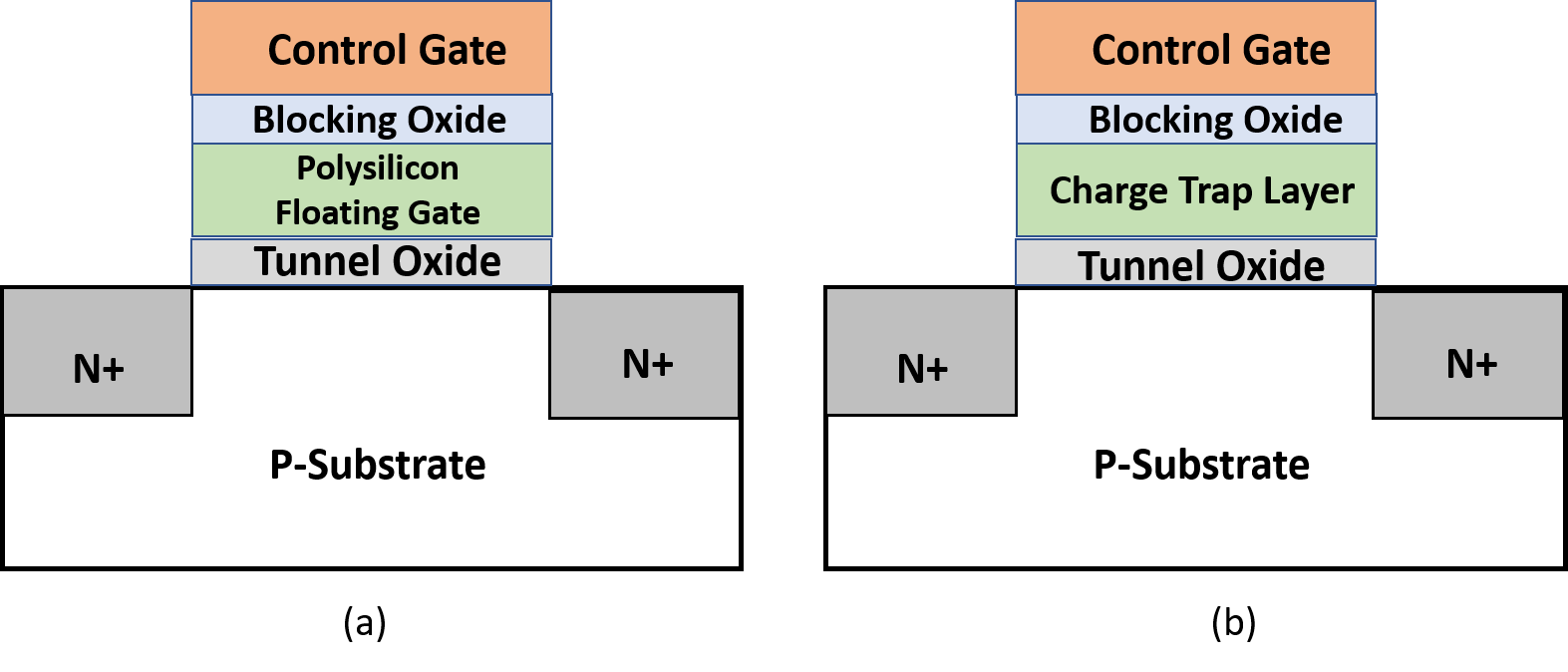
The initial conception of a flash memory cell was a switching transistor that could also store charge or discharge on demand. To do this, a floating gate and an extra insulator layer was inserted between the control gate and the transistor. This floating gate could hold charge or release it based on the voltage applied on the control gate.
Floating gate flash cells were the dominant technology for a long time, until a variation of this topology was introduced called the charge trap flash (CTF) memory cell. Here, a non-conductive silicon nitride layer is substituted in place of the floating gate that can hold charge. Today, this is predominantly used due to better cell endurance, lower leakage and better ease of 3D stacking.
For the rest of this discussion, let us abstract the floating gate, or charge trap, as a “charge storage” layer.
Single Layer Cell (SLC) Flash
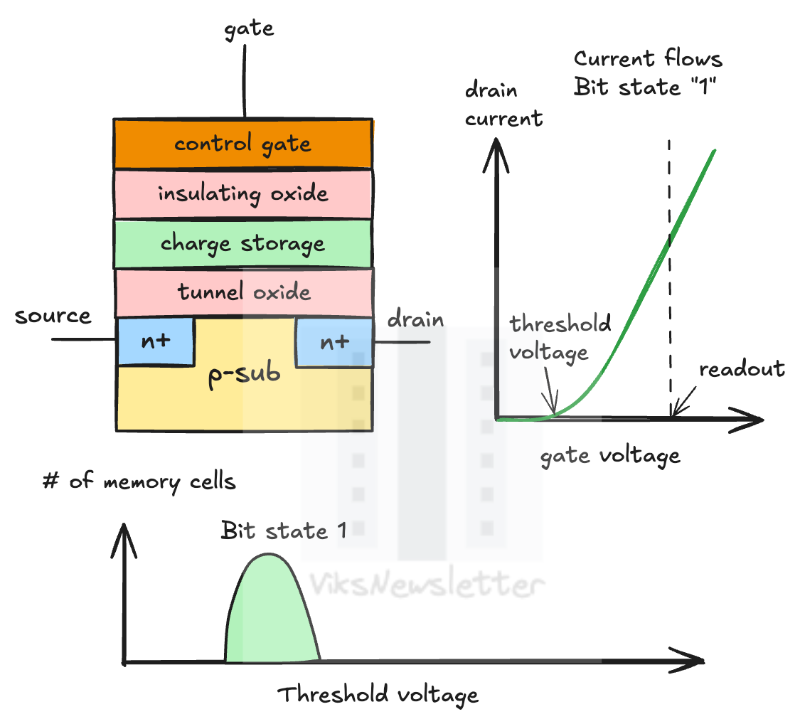
When there is no voltage applied on the control gate, there are no charges stored and the threshold voltage of the transistor is lower than the readout voltage. This means that current can nominally flow through the transistor and represents a default state of ‘1’.
When voltage is applied at the gate, electrons move from the substrate and into the charge storage layer by quantum mechanical tunneling through the gate oxide insulator. This causes the threshold voltage to shift higher. Current can no longer flow at the readout voltage and the cell state is ‘0’.
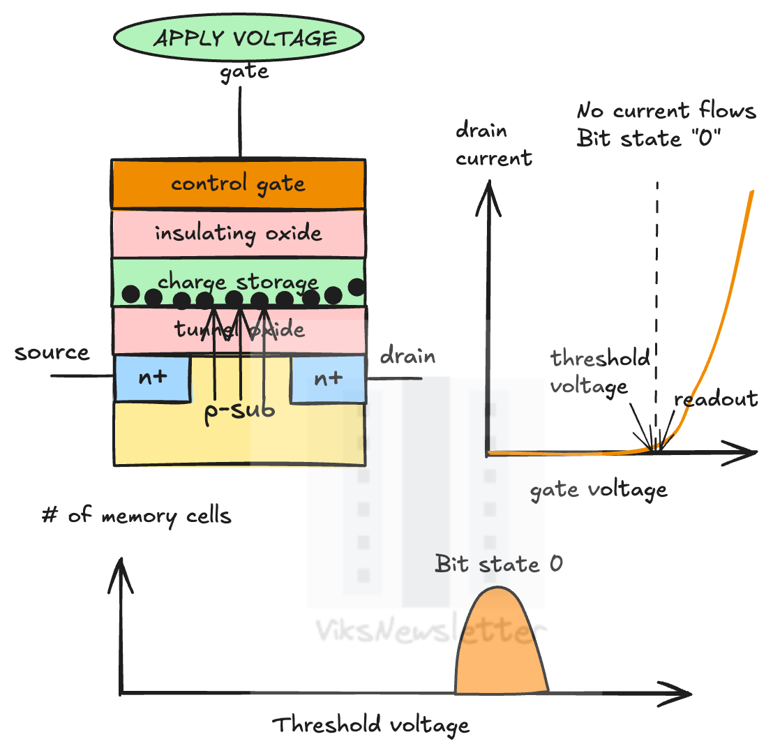
To determine the state of the cell (0 or 1), a sense amplifier is used to estimate the threshold voltage of the transistor by comparing it to a reference voltage. Since only one charge level exists (other than zero charge), this kind of cell is called a single layer cell (SLC). SLC flash is typically fast because only one voltage comparison needs to be made to the reference level.
To program/erase (P/E) the cell, a voltage is applied to the silicon substrate and the electrons are pulled out from the floating gate again through quantum mechanical tunneling. Continuously writing and erasing a NAND cell causes the oxide to break down when electrons constantly keep tunneling through it. This is why NAND flash has endurance limits. SLC flash has the highest endurance of all types we will discuss because a simple cell with just two states puts less stress on the cell during P/E cycle.
MLC, TLC, QLC Flash
There is no fundamental reason the flash cell should stay binary. Threshold voltage shift depends on the amount of charge stored, and multiple bits can be stored in the same cell. This leads to a doubling of memory density in flash cells every time an additional bit is added.
For a 2-bit cell, with four distinct threshold voltages, this is called a multi-level cell (MLC). The idea can be extended to 3-bits or triple level cells (TLC) with 8 voltage levels, 4-bits or quad level cells (QLC) with 16 voltage levels, or even 5-bits or penta level cells (PLC) with 32 voltage levels.
Today, QLC is the production state of the art, while PLC is still in research stages. MLC, TLC, and QLC have increasing drive capacities as more bits are added. The picture below shows a TLC flash cell, which is widely used.
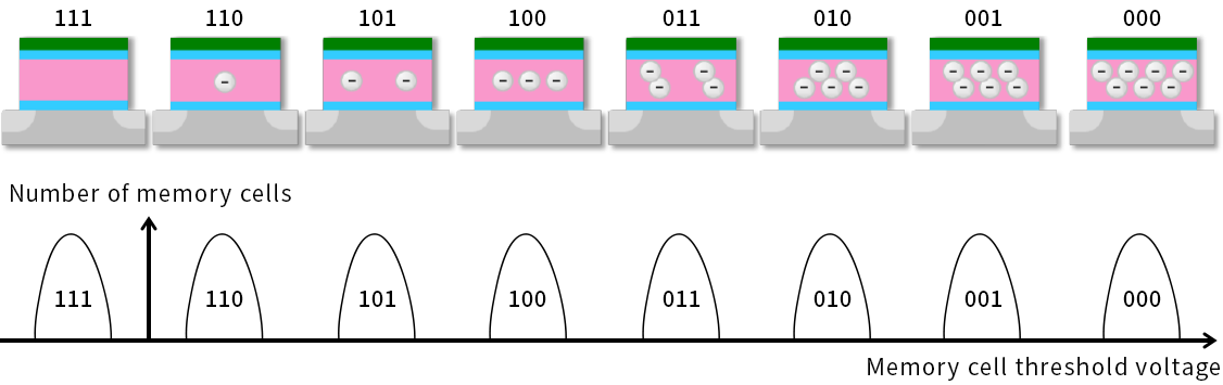
The downside to storing multiple bits in a cell requires charge storage levels to be precisely controlled, and there are many more voltage reference levels that must be determined for every cell. This results in latency, endurance and temperature stability problems.
After the paywall, we will discuss the following:
Latency issues in multi-level NAND cells: Root causes for why higher capacity comes at the cost of higher latency.
Endurance and thermal stability: Fundamental reasons why the multi-level approach results in lower endurance, and also higher sensitivity to temperature.
QLC SSDs for AI workloads: Why this class of SSDs offer incredible storage density, and where it fits compared to HDDs, and TLC SSDs.
CPU requirements for QLC SSDs: Compute requirements when QLC SSDs are used in storage servers.
Testing challenges for QLC SSDs: Fundamental constraints in performance testing.
QLC adoption vs HDDs: What the advent of QLC-based storage systems means for HDD storage.
Market players: A quick rundown of all the competitors on the NAND SSD stage, their market shares, and latest technology updates.