
The Manufacturing Challenge Behind Nvidia’s Plan to Mount AI Chips Directly on PCB Platforms
Is substrate-like PCB technology sufficiently ready to replace ABF substrates that are ubiquitous in AI chips today?

Welcome to a 🔒 subscriber-only deep-dive edition 🔒 of my weekly newsletter. Each week, I help investors, professionals and students stay up-to-date on complex topics, and navigate the semiconductor industry.
If you’re new, start here. As a paid subscriber, you will get additional in-depth content. We also have student discounts and lower pricing for purchasing power parity (see discounts). See here for all the benefits of upgrading your subscription tier!
Nvidia’s AI chips today rely on TSMC’s CoWoS packaging — a mature “chip-on-wafer-on-substrate” flow where a GPU and high-bandwidth memory (HBM) sit on a silicon interposer, then mount onto an ABF-based organic substrate with 15+ routing layers. ABF (Ajinomoto Build-Up Film) is the industry standard for such substrates and a known supply bottleneck considering that the U.S. has no domestic ABF source.
A shift away from ABF would have deep supply-chain and geopolitical implications. This is why Nvidia’s recent exploration of CoWoP (chip-on-wafer-on-platform) technology drew attention in investor circles. CoWoP mounts the interposer directly to a PCB platform, bypassing the ABF substrate entirely. For this to work, PCB fabrication must match the interconnect density of ABF substrates. Can PCB makers deliver the kind of feature sizes, scale, yield and reliability AI accelerators demand?
In this post, we will explore:
The significance of displacing CoWoS: The substrates used in CoWoS have supply chain issues, and not using them has massive implications.
The benefits of moving to CoWoP: Eliminating the IC substrate has advantages in both electrical and thermal performance.
PCB manufacturing processes: The detailed process flows of subtractive and semi-additive PCB manufacturing provides a foundational understand of what is possible for CoWoP.
Substrate-like PCBs: Understanding how IC substrates are currently evolving for CoWoS, and where substrate-like PCBs (first developed for cellphones) fit in.
Can CoWoP be reality? We look at the feasibility of making substrate-like interconnects on PCB by looking at manufacturing capabilities and making some extrapolations.
Read time: 11 mins
If you need a refresher on semiconductor packaging, check out the post below.

The Significance of Displacing CoWoS
A recently leaked slide from Nvidia's internal technical presentation shows that Nvidia is pursuing a new approach to chip packaging on the Grace Rubin 150 (GR150) platform, expected to be released in late 2026. The article released by wallstreetcn.com shows that a new packaging technology called Chip-on-Wafer-on-Platform (or PCB) (CoWoP) is going to be used alongside Chip-on-Wafer-on-Substrate (CoWoS), as a pipe cleaning exercise in GR100, followed by a Process-of-Record (POR) flow in GR150.

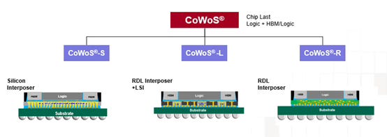
CoWoS® is a TSMC-specific term for the mature packaging technology that forms the basis of AI chips produced by Nvidia. It often involves a logic chip like a CPU or GPU, and high bandwidth memory (HBM), that is placed on an interposer wafer that makes the connections between the CPU or GPU, and HBM. This chip-on-interposer is then mounted on a substrate (in dark green, in the picture below) with BT core material, and Ajinomoto Buildup Films (ABF).
ABF is by far the most commonly used material for such a packaging application, and the availability of high-end ABF substrates has been a supply chain bottleneck before. In the pandemic-era PC boom, Broadcom’s product lead times jumped to 70 weeks due to ABF unavailability. In fact, the Ajinomoto Group controls 98% of the IP licensing rights granted to a handful of East Asian companies which include Unimicron, Nan YA, Ibiden, Shinko, and Kinsus.
The US does not have an independent source of ABF for its advanced packaging needs; it entirely relies on sourcing it externally. In short, ABF sourcing represents a single point of failure for the future of US semiconductors. A recent report by Convergence Analysis, an AI research organization, proposes how US can effectively partner with Japan for ABF to bolster its supply chain.
Alternatively, any packaging advancement that reduces or completely removes the dependence on ABF has major implications for the future of advanced semiconductor packaging. It decreases the reliance of US chips on East Asian companies, and imbalances the supply-demand dynamic especially when the Ajinomoto Group is making investments to increase ABF production.
This is what CoWoP does, and thats why Nvidia’s proposal to use it caused quite a stir.