
🍪 TWiC: TPU v8, Intel Rises Up, Marvell-Polariton
This Week in Chips: Everybody loves a good XPU.

A quick personal update: I parted ways with Qualcomm; and will now be focusing my efforts on thinking, writing, and talking about the semiconductor industry. This is a big step for me, and I’m excited for the future. If there is any interest, I may follow up with a longer post with the thoughts around my decision. Let me know in the comments.
I am pausing subscriptions for just under a week (April 25th - April 30th) since I am leaving for a week’s vacation today. Your existing subscription will extend accordingly, and you will still have access to all paid articles. New paid subscribers cannot sign up in that time. There will be no deep-dive and TWiC next week, but there may be a Semi Doped podcast from the beach. 🌊 Not sure yet.
Substack deep-dive this past week was about a new optical pluggable format called XPO spearheaded by Arista Networks, and how that matters for CPO.

CPUs for agentic AI are becoming hotter, and demand far outstrips supply at the moment. In light of this, I have removed paywalls from my most widely read, and highest revenue generating post ever on this Substack, so more people may have access and get a sample of what kind of content lies behind paywalled deep dives.

I wrote about this just about two months ago, when other sharp analysts like FundaAI were calling out CPU shortages. The deep dive outlines why agentic AI demands more CPUs. Also, the post has been updated to add comparisons to ARM AGI CPU as well.
On the Semi Doped podcast, we spoke about Credo acquiring Dust Photonics, more XPO discussions, and a new AI CPU company - NuvaCore.
We’re also starting up a Substack presence for Semi Doped where Austin and I will write our commentary on industry goings on as a complement to the podcast. Our intentions are to keep this entirely free, less crazy technical, and accessible to a wide range of people interested in keeping a pulse on the semiconductor industry. It’s meant to be easy reading. Do sign up and tell your colleagues!
With all that housekeeping out of the way, let’s get to the news.
Google announces TPU v8 chips and new networking architectures
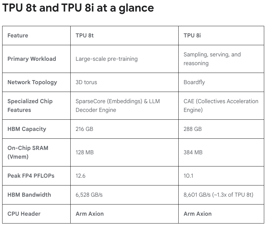
Google Cloud Next is the biggest piece of news this week where the company announced their newest line of TPU chips: v8t for training and v8i for inference. This is the first TPU generation where there are two SKUs with different chip specifications. It is now clear that training and inference have different hardware needs: in both chips and networking.
Few interesting things to note:
HBM capacity on the inference chip is higher than training. Memory bandwidth is critical for inference performance as more people and agents use AI. Training is not really general public facing, and you can build out a datacenter with more GPUs even if lesser HBM exists. It’s still not clear to me why not max out everything.
Look at the on chip SRAM on TPU 8i! It’s 3x higher than the training chip. Having SRAM allows you to automatically provide fast inference without having to use special chips like Groq LPU. The TPU 8i with its SRAM bandwidth can actually decode really fast. I’ve always maintained that having SRAM is the key here, not strange architectures like Groq’s VLIW architecture. In any case, Google TPU’s systolic arrays do provide deterministic behavior like Groq VLIW.
Arm Axion CPUs as the head node. This is a chip developed internally by Google based on Arm architecture. More evidence that ISA is not really that important anymore.
Finally, the networking innovations.
At the scale-out level, Google’s new Virgo architecture replaces their Jupiter network by using Optical Circuit Switches (OCS) with high switch radix. This allows a lot of chips to be connect with just two networking layers, greatly reducing latency.
At the scale-up level, the training chips still use 3D torus. The interference chip networking now goes to a Boardfly approach.
4 TPU 8i chips to a board — connected by copper
8 boards to a rack (also called group) — connected by AEC
36 groups to the pod — connected by OCS
Total 1,152 TPUs per pod
The underlying substrate for all of Google’s TPU networking is OCS. This is a structural change that makes future Google datacenters heavily rely on both optics and copper. I explain the entire networking aspect in-depth on Semi Doped. Look out for the next episode on YouTube.
Intel goes from surviving to thriving
Just a year ago Intel was struggling for existence. TSMC was about to get control of Intel Fabs and help resurrect the business - a brainchild idea of not-quite-loved ex-chairman of the board Frank Yeary. Even Qualcomm allegedly approached Intel for a takeover.
In a riches-to-rags-to-riches story - a comeback story that everybody loves - Intel is now in a position of dominance across three different assets: (1) x86 CPU franchise, (2) advanced packaging, and (3) their massive chip manufacturing network.
The rise of CPUs for agentic AI is a gift that fell in Intel’s lap because it precisely aligns with their core competence. It is up to execution at this point. TSMC’s CoWoS is so bottlenecked that Intel’s EMIB packaging is getting increasingly higher order backlogs. Seemingly, their 18A yields are improving as well. The AI story is playing out because, according to Intel’s latest earnings call, their AI-driven business represents 60% of revenue and grew 40% YoY.
It’s not just CPUs though. Lip-Bu stated on the earnings call that they are “quietly building up the GPU with a new hire” — which refers to Eric Demers being hired as Chief GPU architect earlier this year, who also led Qualcomm’s GPU efforts before he joined Intel.
Lip-Bu also has been smitten by the Elon bug as part of the Terafab project, stating on the earnings call:
We are excited to explore innovative ways to refactor silicon process technology, looking for unconventional ways to improve manufacturing efficiency that will eventually lead to a dynamic improvement in the economics of semiconductor manufacturing.
Sure, you do you — as long as we can get 18A yield up here on earth before we start building fabs in space.
Marvell announces acquisition of Polariton for Plasmonics
You can’t take your eye off the optics ball with all these CPU/TPU distractions. Marvell continues its spree of acquiring photonics companies as it continues its march toward next-gen 3.2T networking, by announcing the acquisition of Polariton Technologies — a Swiss startup.
It’s too late in the week for heavy physics, and we’ll do that in a future deep dive. Let’s look at this cool picture first. This is what Polariton does.

You can send an optical signal through an electro-optic dielectric material sandwiched between two metal electrodes. When you provide electrical 0s and 1s on one of the metal electrodes, the electrons on the metal interact with the light flowing through the dielectric waveguide causing Surface Plasma Polaritons (SPPs). These things affect the phase of the light creating highly effective, and very tiny, phase shift modulators.
The small size of this thing has two advantages:
Low parasitic capacitance, which means you can modulate at high speeds.
Much lower power dissipation
It’s so interesting when wave-particle interaction physics is hitting mainstream applications. I guess we’re really pushing technology now.
Have a great weekend!
Congrats on the change Vik!
I would be extremely interested into the considerations that went into parting ways with Qualcomm - might be kind of cathartic to reflect on while away from the day to day grind.
One thing is for sure, that would take a lot courage. Congratulations man!!!