
Using AI to Break the Black Magic of RF Design
New research funding and emerging tools are setting a new standard for design.

Welcome to the weekday free-edition of this newsletter that is a small idea, an actionable tip, or a short insight that takes less than 5 minutes to read.
On Sundays, I write in-depth technical deep-dives on many aspects of semiconductors and chip design for paid subscribers of this publication. See all the benefits of upgrading your subscription tier!
In case you missed it, here is last Sunday’s deep-dive:

In other news, I gave a talk on “Protocols in Electronic Design” as part of the Summer of Protocols Townhall lecture series; you can check that out here.
Chip design is notoriously difficult.
Designing, manufacturing and getting stuff to work at scale is an incredibly difficult task that often relies on the intuition of experts. Today, the industry is looking for a way to speed up this process.
According to Devansh’s analysis, Google saves approximately $3.6 million per chip through AlphaChip, a reinforcement learning-based layout design tool. In an earlier post, I explained how we are starting to vibe our way through chip design, and how reinforcement learning is being used to design RF power amplifiers.
Last week, Natcast — a non-profit entity created by the US Department of Commerce — awarded $30 million to further the use of AI in RFIC design.
Let’s unpack why, what’s out there already and who is working on it. 👇🏽
The Complexity of RFIC Design
RFIC design remains a manual, expertise-heavy process, often requiring years of experience to navigate complex trade-offs. Chip design cycles often take 3-4 months from inception to tapeout, and there’s no guarantee of first-pass success. RF design is often referred to as “black magic” simply because of the deep insight required to make the right design decisions.
Compared to digital chips, RFIC designs often have only a few dozen transistors including bias circuits. The difficulty of the design process stems from the complex interactions between various parts of the design.
Electromagnetic fields from on-chip inductors couple with other inductors.
Ground planes must provide low impedance return paths.
Routing parasitics (resistive, capacitive and inductive) between every element on chip must be carefully accounted for.
An additional challenge is that the chip’s packaging significantly affects RFIC performance and must be accounted for early in the design process. A chip-package co-simulation often requires extensive electromagnetic simulations which is a time consuming process.
Why the Industry Needs Change
It’s not only time-to-market that is important for companies, but also the cost of hiring a sufficiently trained workforce. There’s always talk of talent shortage, but the reality is that semiconductor jobs are failing to attract the next generation. On the flip side, I’ve also explained how companies make it needlessly difficult for candidates to enter the workforce.
AI-enabled RFIC design flows are a quick solution to the workforce problem.
Much of the design exploration and optimization can be done by machines, leaving the higher levels of system abstractions to human designers. This is not as bad as it seems; AI isn’t replacing design jobs—it’s reshaping them. Automating away the grunt work of IC design and making quick iterations is beneficial for everybody. This allows junior engineers to tackle more interesting problems instead of being delegated to be simulation monkeys jigsawing IP reuse pieces together.
AI-Driven Design Using RFIC-GPT
One important distinction to make is that generic LLMs are useless for the most part when it comes to domain-specific IC design. I tried unsuccessfully to get ChatGPT to create a simple cascode low-noise amplifier design, and create a netlist that I could simulate. It failed miserably; it could not even stack two transistors in a cascode topology. If you happen to know how to do this right, write to me and let me know.
AI frameworks need to be trained on how to do RFIC design before they can be useful. One such tool available online today is RFIC-GPT, which looks really interesting and is available to try for free online.
I, of course, tried the cascode LNA design example again. Here are my inputs to the online form, which are quite representative of an amplifier for handheld cellular applications.
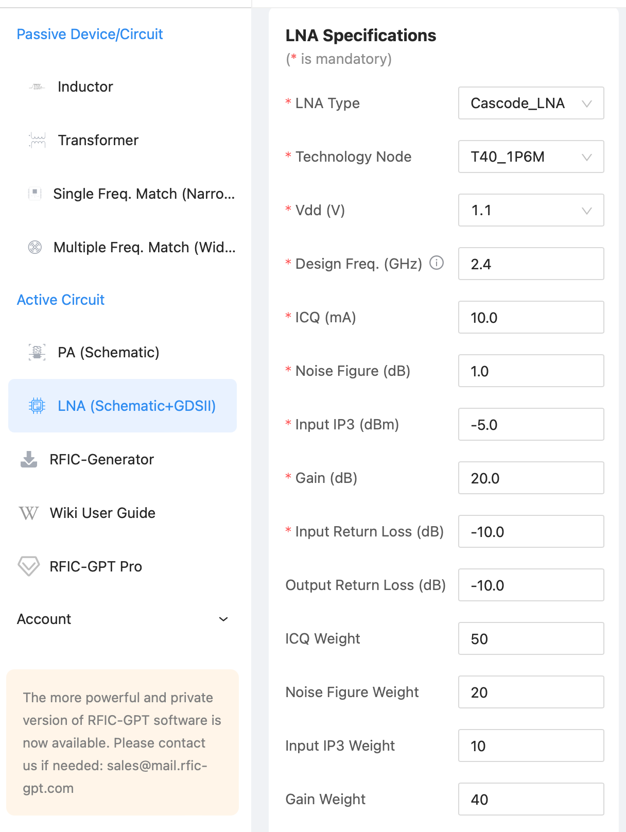
I intentionally weighted the current requirement (ICQ) higher because that is often non-negotiable from a system point of view. Gain is the next highest priority. Noise and linearity specifications were lower down the list. The design process took about two minutes, but here are the options I got and the design is guaranteed for stability too! (I did not check this.)
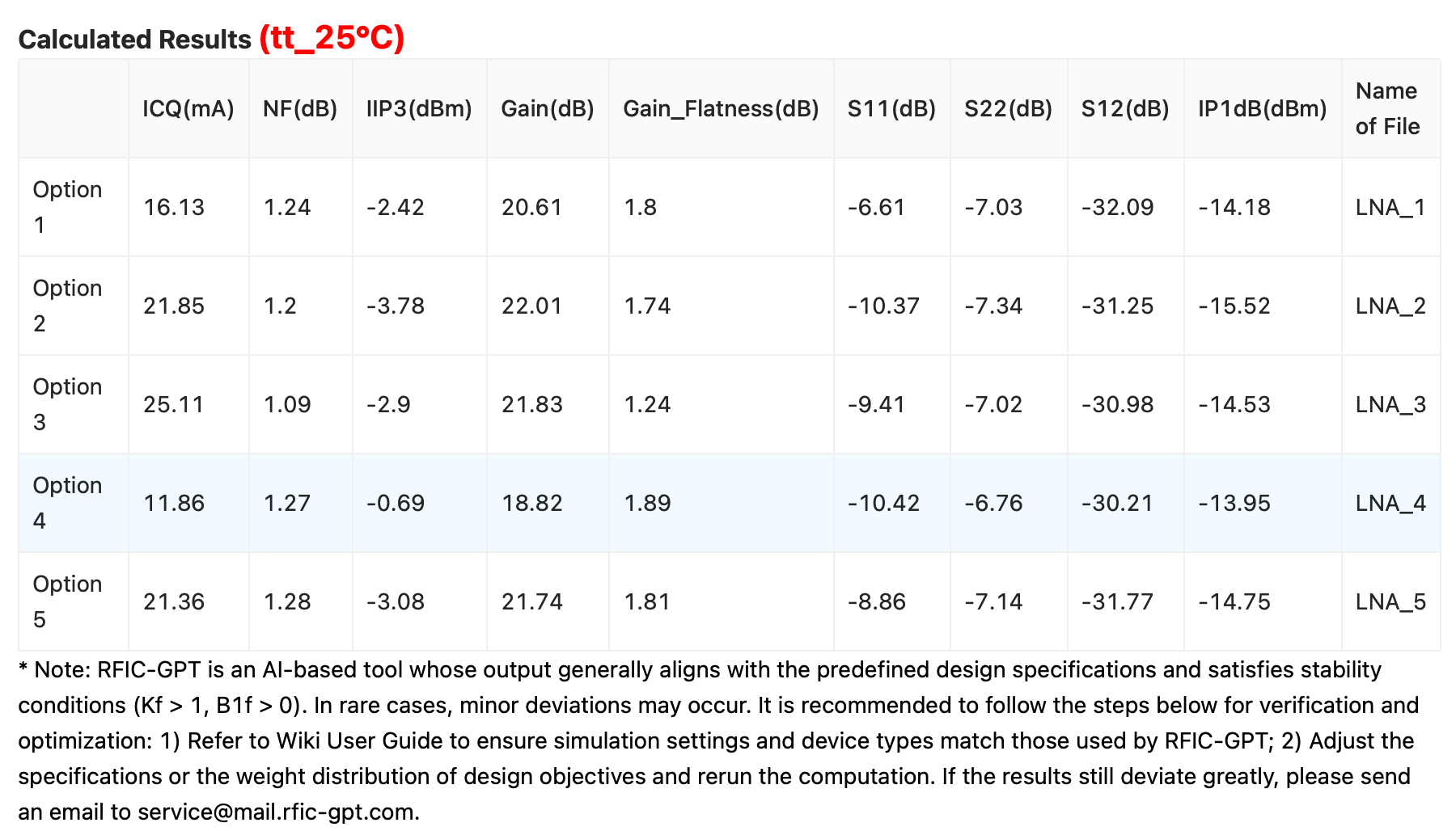
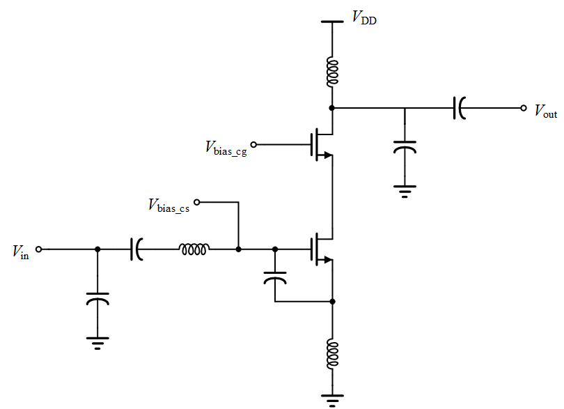
Of these, option 4 looks like a reasonable starting point. The bias current is closest to what I want and the gain is close. The input matching is reasonable, but the output match is not as good as I’d like. I’m sure I’ll be able to iterate on these specifications better with a few attempts at this process. The topology of the schematic is a familiar cascode LNA — for those who’ve done this sort of thing before.
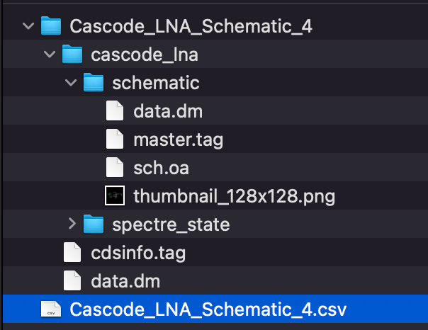
The tool allows me to download the schematic one-time free of charge. It’s pretty neat that they provide a Cadence Virtuoso-compatible open-access schematic and a spectre simulation state to go with it. I can only show you the folder structure because I cannot use my company’s resources to show you the actual schematic. There is a GDSII-ready layout also available but costs $60 to download — which I did not pay. Maybe I’ll contact the developers and ask them if they can provide me an extended demo that I can play around more with and then write about.
The important take-away is that a starting point for LNA design can be generated for $60 and in a few minutes. There is a serious value proposition here for a company which already spends millions on license fees and personnel. Speeding up design flows like this is a no-brainer in terms of cost-benefit trade-off.
They have a downloadable RFIC Generator tool that can be integrated into Cadence Virtuoso and used for GPT-based synthesis of inductors and transformers which can be immensely useful. They also have a Pro version for commercial use. You can read the whole documentation here.
Research Projects Leading the Charge
RFIC-GPT is a simple demonstration of what is possible with AI-enabled design workflows for RF engineering. Advancements in this field can greatly enhance product development speed and quality.
The $30 million R&D contract awarded by Natcast, which oversees the U.S. National Semiconductor Technology Center (NSTC), is split equally between three key players as part of the AI-Driven RFIC (AIDRFIC) program:
Keysight Technologies: AI for Accelerating RFIC Design Efficiency, Innovation, and Optimization for U.S. Competitiveness
IMAGINE (Princeton University): Utilizing generative AI and inverse methods to automate the RFIC design process from specifications to layout, uncovering novel design spaces.
GENIE-RFIC (University of Texas, Austin): Developing AI-driven tools for rapid “inverse” design of both CMOS and GaN RFICs, aiming to discover non-intuitive, high-performance solutions.
Another noteworthy research team (not funded by Natcast) is being led by Prof. Fabio Passos from the University of Lisbon, Portugal. The team’s paper on fully automated mm-wave LNA design is interesting to say the least.
I’ll be looking forward to published work from all these entities in the future, and more so at the upcoming 2025 International Microwave Symposium.
Further Reading
If you’re interested in the field of RFIC design, here are some previous posts I recommend:

